Microfluidic device having hydrophilic microchannels

a microfluidic device and microchannel technology, applied in the field of microfluidic devices, can solve the problems of large space requirements for samples and equipment, large space requirements for screening large numbers of samples using existing parallel screening methods, and inability to meet the requirements of sample and equipment, and achieve the effect of rapid flow rate of test fluids

Inactive Publication Date: 2007-06-21
3M INNOVATIVE PROPERTIES CO
View PDF14 Cites 75 Cited by
  • Summary
  • Abstract
  • Description
  • Claims
  • Application Information

AI Technical Summary

Benefits of technology

[0005] The present invention relates to a microfluidic device that includes a multi-layer film and a microchannel extending through the multi-layer film, where the microchannel has a perimeter surface. The multi-layer film includes a conductive layer and a polymeric layer disposed adjacent the conductive layer. The microfluidic device also includes a hydrophilic layer disposed on the perimeter surface of the microchannel, where the hydrophilic layer comprises at least about 20% by weight silicon and at least about 40% by weight oxygen. The hydrophilic layer allows for rapid flow rates of test fluids through the microchannel of the microfluidic device.

Problems solved by technology

Despite improvements in parallel screening methods and other technological advances, such as robotics and high throughput detection systems, current screening methods still have a number of associated problems.
For example, screening large numbers of samples using existing parallel screening methods have large space requirements to accommodate the samples and equipment.
Available reaction volumes are often very small due to limited availability of the compound to be identified.
Such small volumes can lead to errors associated with fluid handling and measurement (e.g., due to evaporation and dispensing errors).
Additionally, fluid-handling equipment and methods are typically unable to handle these small volumes with acceptable accuracy.
However, microfluidic devices optimized for sensor sensitivity are generally not sufficiently hydrophilic to allow the test fluids to flow through the microchannels and across the electrodes in reasonable test times.

Method used


Image

  • Microfluidic device having hydrophilic microchannels
  • Microfluidic device having hydrophilic microchannels
  • Microfluidic device having hydrophilic microchannels

Examples


example 1

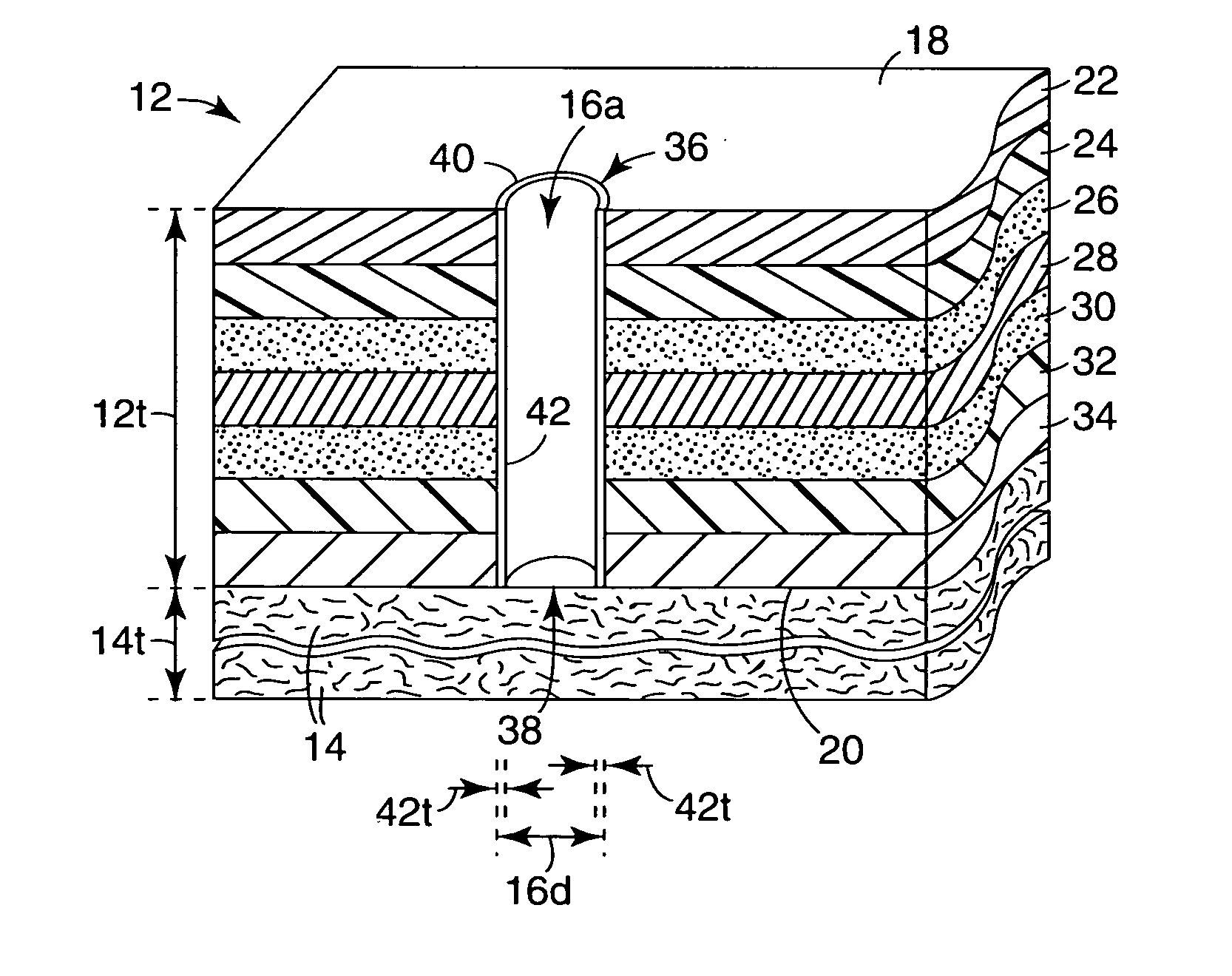
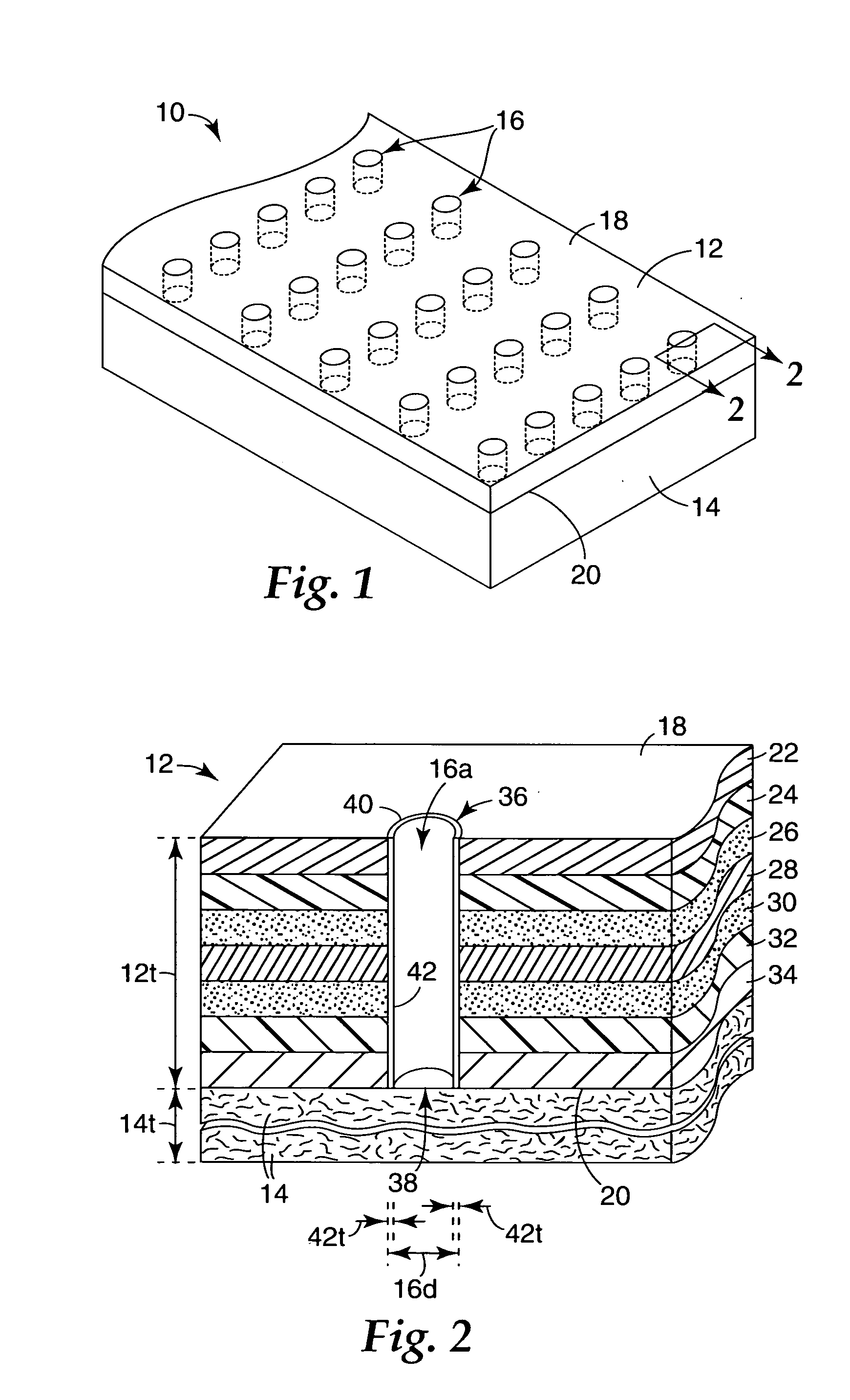
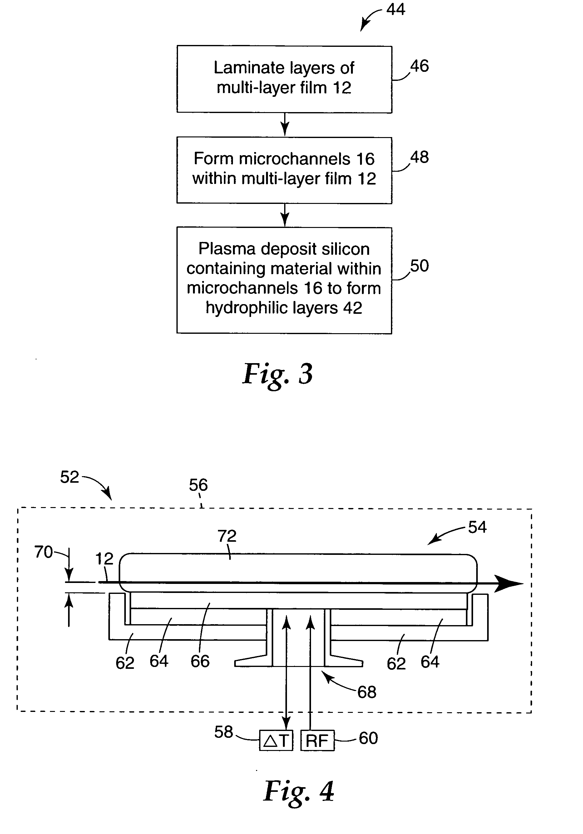
[0059] The microfluidic device of Example 1 included a DLG-based hydrophilic layer without the use of an absorbent layer. The microfluidic device was formed by the following procedure. A pair of single-clad copper / polyimide films were laminated to a single one-ounce copper core sheet with the use of polyimide adhesive films. The resulting multi-layer film resembled the seven-layer film arrangement shown in FIG. 2. Each of the single-clad copper / polyimide films had a copper layer thickness of 18 micrometers and a polyimide layer thickness of 25 micrometers. The copper core sheet and the polyimide adhesive films each had layer thicknesses of 35 micrometers. The two outer copper layers were then plated with copper up to 25 micrometers and then flash plated with 5 micrometers of gold. The layer thickness of the overall multi-layer film was about 200 micrometers, and the surface areas of the top and bottom surfaces of the multi-layer film were 16.7 millimeters×16.7 millimeters (taken in ...

example 2

[0064] The microfluidic device of Example 2 included the microfluidic device of Example 1, where a non-woven pad was laminated to the microfluidic device to function as an absorbent layer.

example 3

[0065] The microfluidic device of Example 3 was formed by the same procedure as discussed above for the microfluidic device of Example 1, except that the TMS flow rate was 50 sccm, the pressure was 50 milliTorr, and the treatment time of the multi-layer film in the TMS / O2 plasma was five seconds. After the plasma deposition process, a non-woven pad was laminated to the microfluidic device to function as an absorbent layer.


PUM

PropertyMeasurementUnit
dielectric constantsaaaaaaaaaa
thicknessesaaaaaaaaaa

Abstract

A microfluidic device comprising a multi-layer film having a conductive layer and a polymeric layer disposed adjacent the conductive layer, a microchannel extending through the multi-layer film, where the microchannel has a perimeter surface, and a hydrophilic layer disposed on the perimeter surface of the microchannel. The hydrophilic layer comprises at least about 20% by weight silicon and at least about 40% by weight oxygen.

Description

BACKGROUND [0001] The present invention relates to microfluidic devices for use in diagnostic applications. In particular, the present invention relates to microfluidic devices having hydrophilic microchannels for use in miniaturized analysis systems. [0002] Diagnostic applications such as medical diagnostics, forensics, genomics, environmental monitoring, and contaminant testing often require routine repetitive testing for detection and identification of chemical compounds. Typically, parallel screening methodologies are used to analyze the large volume of samples in these various fields. Despite improvements in parallel screening methods and other technological advances, such as robotics and high throughput detection systems, current screening methods still have a number of associated problems. For example, screening large numbers of samples using existing parallel screening methods have large space requirements to accommodate the samples and equipment. [0003] Available reaction v...

Claims


Application Information

Patent Timeline
Patent Type & Authority Applications(United States)
IPC IPC(8): B32B3/10
CPCB01L3/5025Y10T428/24322B01L3/502746B01L2300/0645B01L2300/069B01L2300/0887B01L2300/161B01L2400/0406B01L2400/088B32B3/266B32B15/08B32B23/02B32B27/08B32B27/28C23C16/045B32B5/022B32B5/08B32B15/14B32B15/20B32B27/281B32B2255/10B32B2255/20B32B2255/24B32B2262/0246B32B2262/04B32B2262/14B32B2307/202B32B2307/726B32B2307/728B32B2457/00B01L3/502707
Inventor SOMASIRI, NANAYAKKARA L.D.DAVID, MOSES M.
Owner 3M INNOVATIVE PROPERTIES CO
Why Eureka
Try Eureka