Dispersed growth of nanotubes on a substrate

a technology of nanotubes and substrates, applied in the field of nanostructure dispersions, can solve the problems of poor contact deposition and adhesion, difficult to achieve the density of nanotubes needed to reliably make contact with the electrodes, and not a process that will be useful

Inactive Publication Date: 2007-06-21
NANOMIX
View PDF2 Cites 12 Cited by
  • Summary
  • Abstract
  • Description
  • Claims
  • Application Information

AI Technical Summary

Benefits of technology

[0018] In another embodiment, an array of nanostructure devices is provided. The array of devices includes a substrate, a dispersion of nanostructures disposed discontinuously on the substrate and an array of electrodes in contact with the dispersion of nanostructures. The substrate can be made of materials such as silicon, silicon oxides, silicon nitride, alumina, or quartz. Preferably, the nanostructures are nanotubes or nanowires. Preferably, the dispersion of nanostructures is approximately planar and substantially in contact with the substrate. The dispersion of nanostructures can contain carbon, silicon, germanium, arsenic, gallium, aluminum, boron, phosphorous, indium, tin, molybdenum, tungsten, vanadium, sulfur, selenium, and / or tellurium. The dispersion of nanostructures can include regions of nanostructures interspersed with areas containing no nanostructures. Regions containing nanostructures can provide electrical communication between two or more electrodes.

Problems solved by technology

But, it is difficult to achieve the nanotube density necessary to make contact to the electrodes reliably, even after many drops have been deposited.
This is not a process that will be useful for large-scale manufacture of nanotube devices.
Also, the surface of the catalyst is very rough, which would cause poor contact deposition and adhesion, not compatible with semiconductor processing, and would therefore not be manufacturable.
Current methods for producing nanotubes and devices, such as those described above, are not compatible with low-cost, mass-production manufacturing, nor are they likely to yield devices that have good, long-term reliability.

Method used


Image

  • Dispersed growth of nanotubes on a substrate
  • Dispersed growth of nanotubes on a substrate
  • Dispersed growth of nanotubes on a substrate

Examples


Embodiment Construction

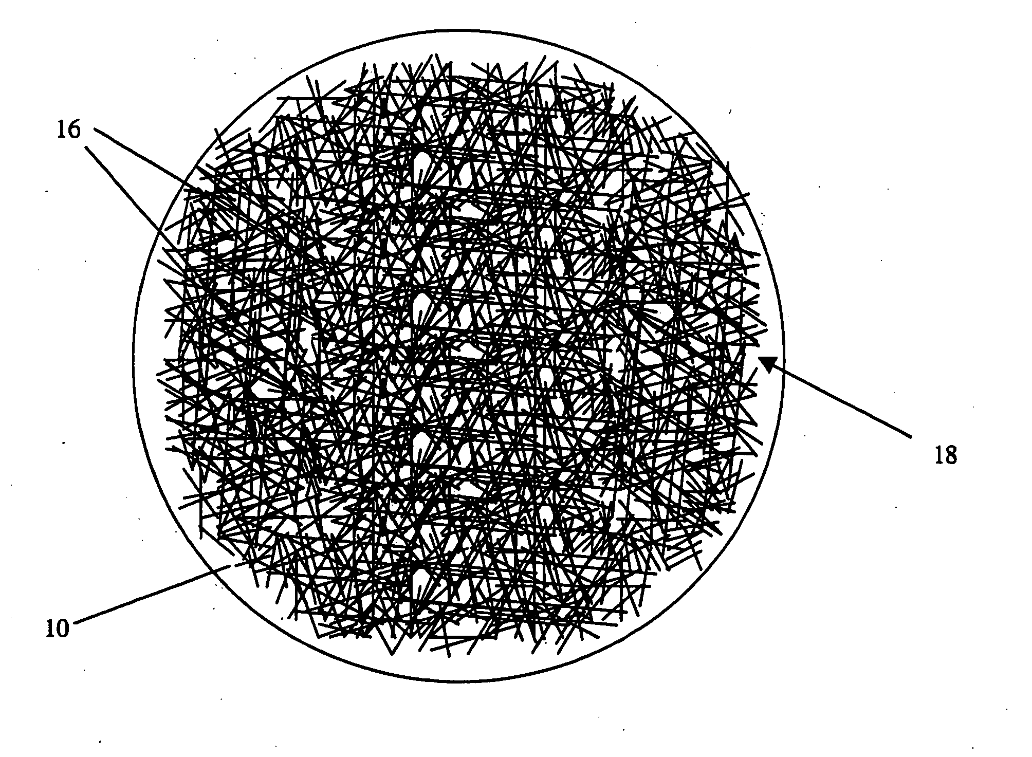
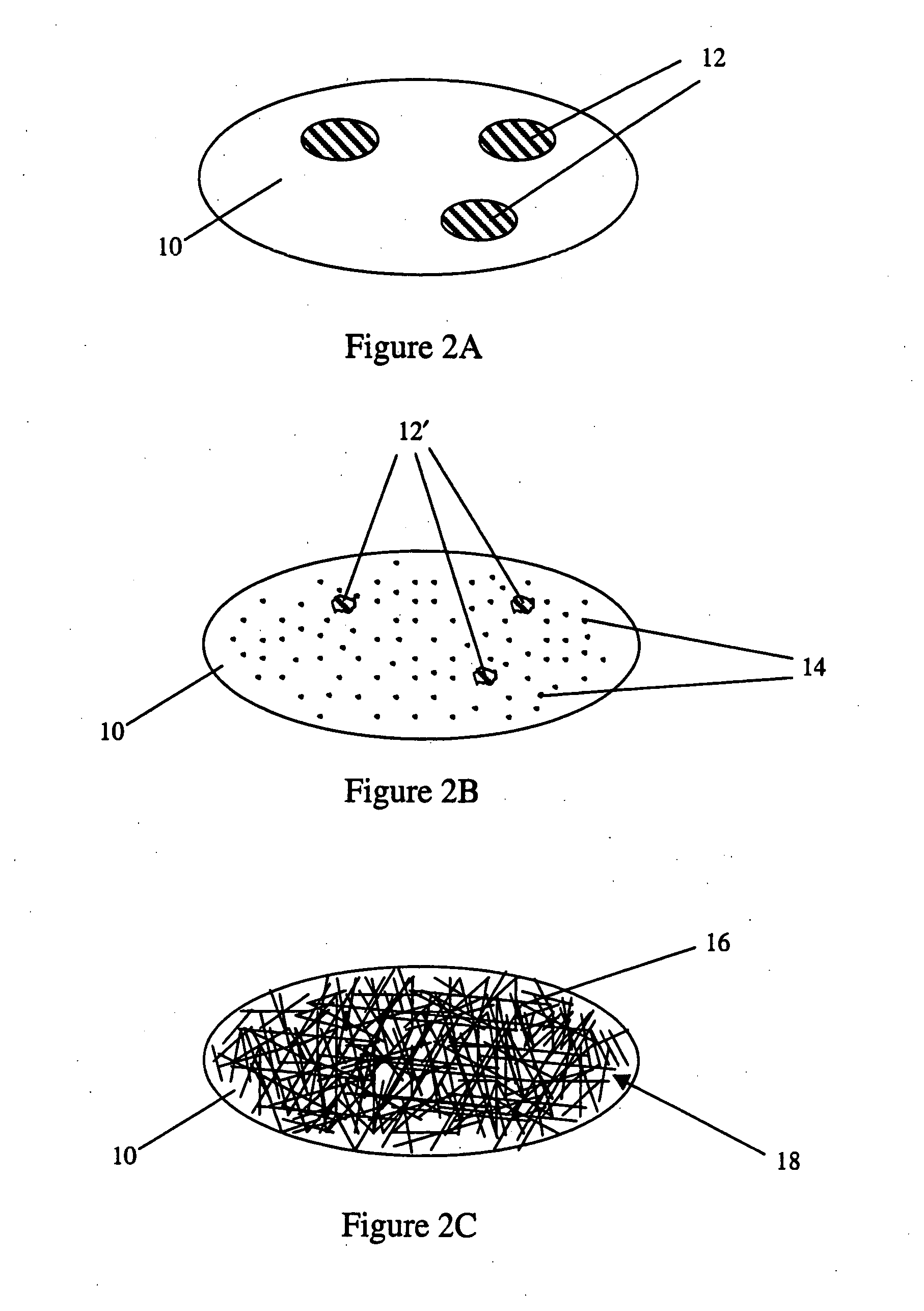
[0029] In order to make full use of nanostructures in device technology, it will be necessary to find ways to manufacture the devices that are efficient and cost-effective. Much of the work that has gone into developing nanostructure devices has been at the laboratory level using methods that are not appropriate for large-scale manufacturing. If a high density, good quality, random dispersion of individual nanostructures can be formed on a semiconductor substrate, then a “statistical,” rather than a “localized” approach to nanostructure device fabrication can be used. In the “statistical” approach, electrical contacts can be placed anywhere on the dispersion of individual nanostructures to form devices. It is not necessary to make a specific correspondence between electrode position and nanostructure position as in the “localized” approach, because the high density dispersion of nanostructures ensures that any two or more electrodes placed thereon can form a complete electrical circ...


PUM

PropertyMeasurementUnit
sizeaaaaaaaaaa
sizeaaaaaaaaaa
sizeaaaaaaaaaa

Abstract

Methods of forming a dispersion of nanostructures, a distribution of carbon nanotubes, and an array of nanostructure devices are described. The methods involve providing a substrate, applying growth promoter to at least a portion of the substrate, exposing the substrate and the growth promoter to a plasma, and forming a dispersion of nanostructures from the growth promoter after the plasma exposure. Exposing the substrate and the growth promoter to a plasma disperses at least a portion of the growth promoter as distinct, isolated growth promoter areas over the substrate. Preferably, the growth promoter areas are nanoparticles between about 1 nm and 50 nm in size and they are dispersed approximately uniformly over the substrate. An array of nanostructure devices is also described. The array of devices includes a substrate, a dispersion of nanostructures disposed discontinuously on the substrate and an array of electrodes in contact with the dispersion of nanostructures. The nanostructures may be nanotubes or nanowires. Preferably, the dispersion of nanostructures is approximately planar and substantially in contact with the substrate. Regions containing nanostructures can provide electrical communication between two or more electrodes.

Description

CROSS-REFERENCE TO RELATED APPLICATIONS [0001] This application is a divisional application of U.S. patent application Ser. No. 10 / 177,929, filed Jun. 21, 2002, which is hereby incorporated by reference in its entirety as if fully set forth.BACKGROUND OF THE INVENTION [0002] 1. Field of the Invention [0003] This invention relates generally to formation of nanostructure dispersions, and, more specifically, to methods for forming nanotube dispersions on substrates and for forming nanostructure devices. [0004] 2. Description of the Related Art [0005] There has been much interest in using nanostructures as active components in electronic devices. The basic idea is to connect electrodes to nanostructures, thus forming an electric circuit. The nanostructures can be biased with a gate electrode to form devices such as transistors. [0006] One approach has been to make the nanotubes first and then place them onto a prepared substrate. Conventionally, the nanotubes are formed either by arc-di...

Claims


Application Information

Patent Timeline
Patent Type & Authority Applications(United States)
IPC IPC(8): D01F9/12D01F9/127H01M
CPCB82Y10/00B82Y30/00D01F9/12D01F9/127H01L29/1025H01L29/12H01L29/66409H01L29/772
Inventor GABRIEL, JEAN-CHRISTOPHE P.BRADLEY, KEITHCOLLINS, PHILIP G.
Owner NANOMIX
Why Eureka
Try Eureka