Local interconnection method and structure for use in semiconductor device

a local interconnection and semiconductor technology, applied in the field of manufacturing of semiconductor devices, can solve the problems of inability to obtain contact patterning of such a size, difficult to guarantee a determined thickness margin, and inability to continue to increase integration, so as to reduce the number of process steps required, reduce the manufacturing cost of semiconductor devices, and increase the manufacturing yield

Inactive Publication Date: 2007-06-21
SAMSUNG ELECTRONICS CO LTD
View PDF8 Cites 10 Cited by
  • Summary
  • Abstract
  • Description
  • Claims
  • Application Information

AI Technical Summary

Benefits of technology

[0027] Still another feature of embodiments of the present invention is to provide a local interconnection structure and a method of forming the wiring structure in a semiconductor device, which is capable of reducing or fundamentally preventing a short caused by a contact between a local interconnection layer and an active region of a semiconductor device.
[0029] Another feature of embodiments of the present invention is to provide a local interconnection wire forming method to reduce the number of process steps required for a formation of interconnection wire and thus reduce a manufacturing cost of semiconductor devices.
[0030] An additional feature of embodiments of the present invention is to provide a local interconnection wire forming method and structure capable of increasing a manufacturing yield and enhancing a performance of the interconnection wire in a semiconductor device.

Problems solved by technology

The continuously increasing integration is limited by the size of local interconnection wiring process of locally connecting conductive layers.
For example, a contact of tungsten (W) matter having a pitch of 0.20 μm should be formed when a high integration semiconductor device has a design rule for an interval under 0.10 μm therefore, but it is actually impossible to obtain a contact patterning of such a size even if the current advanced technique of lithography is used.
If the interlayer insulation film 12 becomes too thin by the excessive etching, it will be difficult to guarantee a determined thickness margin.
Although the SiN / SiON film 15 was conventionally deposited to be used as the hard mask, it was still very difficult to substantially reduce the occurrence probability of short between the local interconnection layer 16 and the active region 9 caused by excessive etching of the interlayer insulation film 12 formed on the active region 9.
This increases the manufacturing cost for semiconductor devices.
If the interlayer insulation film 12 is thinned by the excessive etching, a given thickness margin cannot be guaranteed.
In order to solve this problem, a local interconnection wire for locally connecting between gate electrodes and between active regions is formed, but if an interlayer insulation film is thinned by an excessive etching, a determined thickness margin cannot be guaranteed and this brings about a high occurrence probability for a short between a local interconnection layer and an upper part of active region.
However, an etching process for the hard mask constructed of the SiN / SiON film, etc. and a flattening process for the local interconnection layer are needed separately due to the hard mask formation process, thus there are a large number of process steps.
This increases the manufacturing cost of semiconductor devices.

Method used


Image

  • Local interconnection method and structure for use in semiconductor device
  • Local interconnection method and structure for use in semiconductor device
  • Local interconnection method and structure for use in semiconductor device

Examples


Embodiment Construction

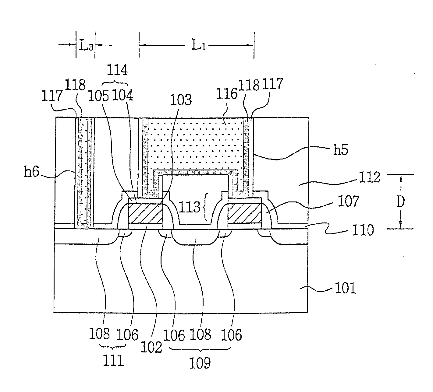
[0038] According to exemplary embodiments of the present invention, local interconnection structure and method will be described with reference to FIGS. 3 through 6.

[0039] It will be understood by those skilled in the art that the present invention can be embodied by numerous different types and is not limited to the following described embodiments. The following various embodiments are exemplary in nature. Accordingly, details of like components have been omitted so that the invention can be clearly presented.

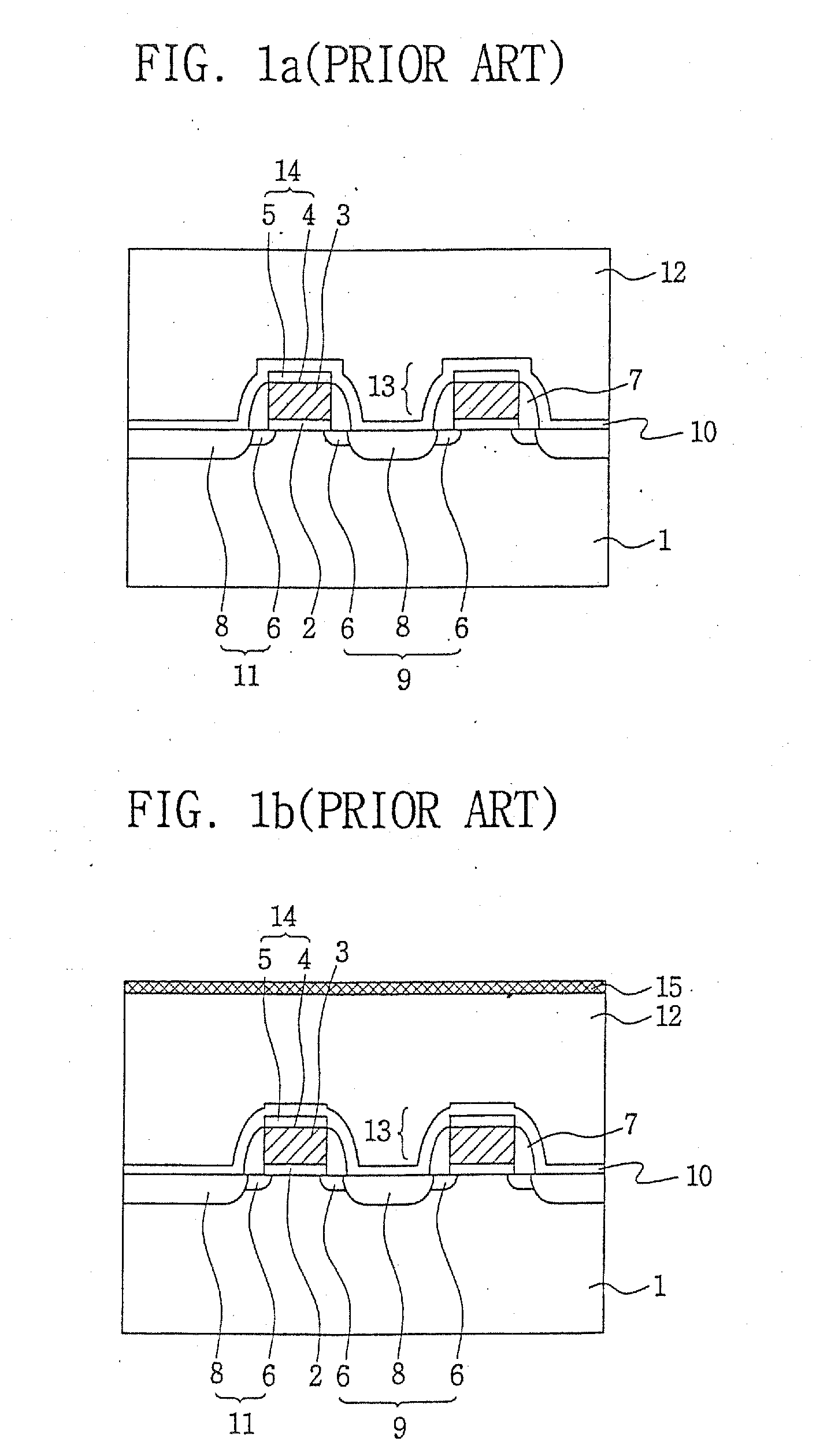
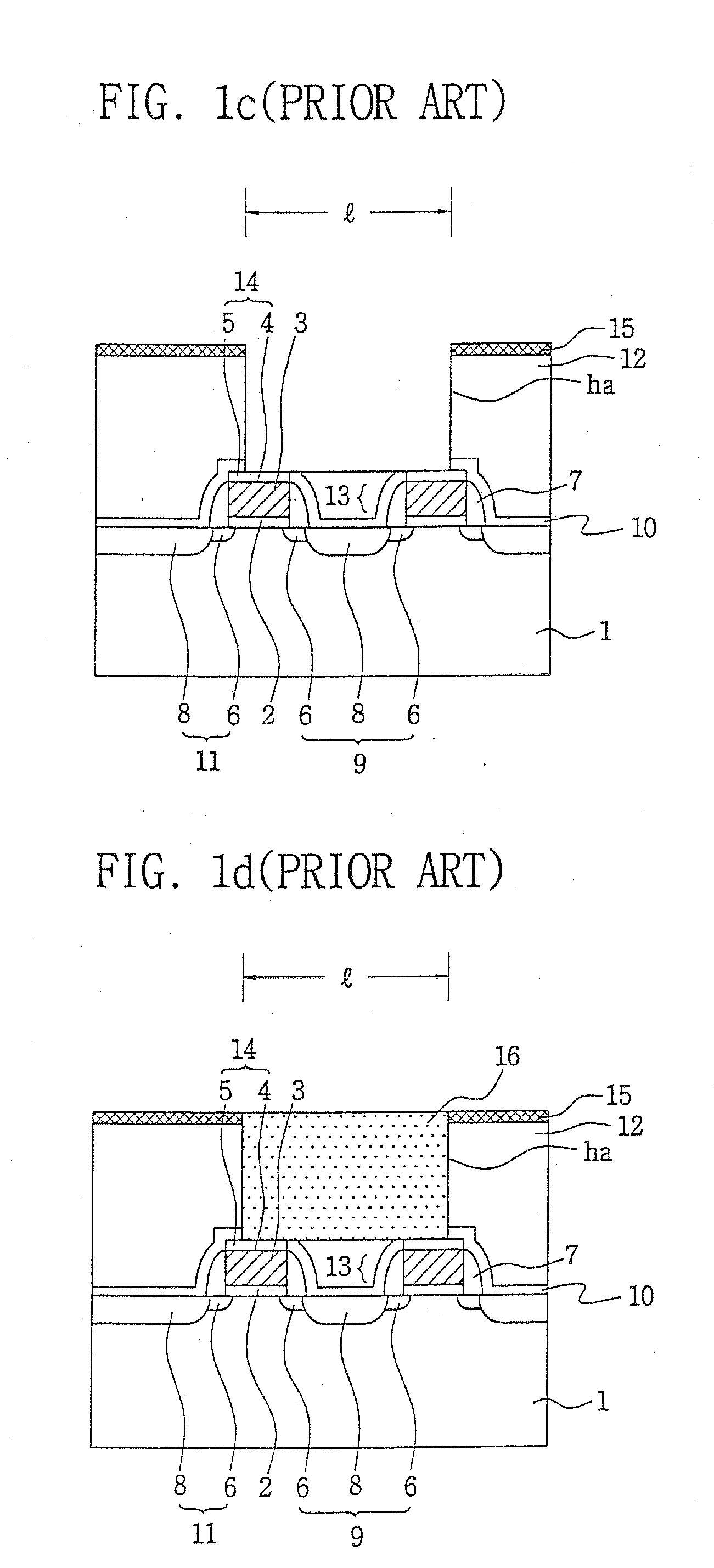
[0040]FIGS. 3a through 3e are cross-sectional views showing a sequential process of local interconnection wire according to exemplary embodiments of the present invention. FIGS. 4a through 4d illustrate other exemplary embodiments, FIGS. 5a and 5b illustrate still other exemplary embodiments, and FIGS. 6a and 6b illustrate yet other exemplary embodiments. These figures are all cross-sectional views each illustrating a sequential process of local interconnection wire.

[0041] ...


PUM


Abstract

A local interconnection wiring structure method for forming the same reduces the likelihood of a short between a local interconnection layer of gate electrodes and an active region by forming a common aperture so as to have a determined aperture between the local interconnection layer and the active region on an insulation film of a semiconductor substrate. Methods of forming the local interconnection wire can include forming a first etching mask pattern that has a size longer than a length between inner ends of adjacent gate electrodes formed on a semiconductor substrate and covered with an insulation film. The etching mask simultaneously has a length the same as or shorter than the length between outer ends of the gate electrodes. The insulation film exposed in the first etching mask pattern is subsequently etched so that the insulation film remains higher than a highest height of the gate electrodes, so as to form a recess pattern. The first etching mask pattern is then removed and a second etching mask pattern is formed so as to partially expose the insulation film provided within the recess pattern. The insulation film within the recess pattern is etched to form apertures for exposing a partial surface of the gate electrodes. The second etching mask pattern is then removed. The recess pattern and the apertures are then filled with conductive material to form a local interconnection layer for connecting between the gate electrodes.

Description

[0001] This is a Divisional of U.S. patent application Ser. No. 10 / 861,863, filed on Jun. 4, 2004, now pending, which claims priority from Korean Patent Application No. 2003-35875, filed on Jun. 4, 2003, the entire contents of which are hereby incorporated by reference.FIELD OF THE INVENTION [0002] This disclosure relates to a manufacturing of semiconductor devices, and more particularly, to a local interconnection structure and method of connecting between conductive layers such as an active region or a gate electrode of a semiconductor device, etc. BACKGROUND OF THE INVENTION [0003] Requirements for lower electricity consumption and higher performance semiconductor devices has gradually increased. This has brought about continuous research and development to obtain high integration and high-speed operation of semiconductor devices. The continuously increasing integration is limited by the size of local interconnection wiring process of locally connecting conductive layers. [0004] ...

Claims


Application Information

Patent Timeline
Patent Type & Authority Applications(United States)
IPC IPC(8): H01L21/4763H01L21/28H01L21/44H01L21/768
CPCH01L21/76807H01L21/76808H01L21/76831H01L21/76895H01L21/28
Inventor KWON, SUNG-UNKO, YONG-SUN
Owner SAMSUNG ELECTRONICS CO LTD
Why Eureka
Try Eureka