Interconnect manufacturing process

Inactive Publication Date: 2009-04-02
NAN YA TECH
View PDF5 Cites 0 Cited by
  • Summary
  • Abstract
  • Description
  • Claims
  • Application Information

AI Technical Summary

Benefits of technology

[0013]Accordingly, the present invention is directed to an interconnect process, which prevents a contact from being in contact with a gate to cause shor

Problems solved by technology

When integrity of an integrated circuit (IC) is increased, a surface of a chip cannot provide enough area for placing

Method used


Image

  • Interconnect manufacturing process
  • Interconnect manufacturing process
  • Interconnect manufacturing process

Examples


Example

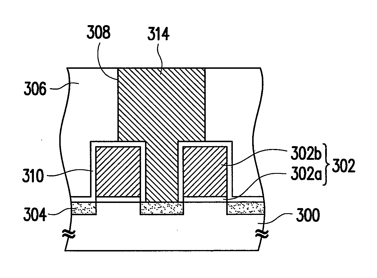
[0030]FIGS. 2A to 2D are cross-sectional views of processes of the interconnect process according to an embodiment of the present invention.

[0031]First, referring to FIG. 2A, a substrate 300 is provided. The substrate 300 has gate structures 302 thereon. Each of the gate structure 302 includes a gate dielectric layer 302a located on the substrate 300 and a gate 302b located on the gate dielectric layer 302a. Moreover, doped regions 304 are disposed in the substrate 300 and respectively located between two adjacent gate structures 302, so as to serve as a source / drain region.

[0032]Referring to FIG. 2B, a liner 310 is conformally formed on the substrate 300. The material of the liner 310 is, for example, silicon oxide, and the liner 310 is formed by, for example, a chemical vapor deposition (CVD) process. A dielectric layer 306 is formed on the substrate 300. The material of the dielectric layer 306 is, for example, silicon oxide, and the dielectric layer 306 is formed by, for example...


PUM


Abstract

An interconnect process is provided. A substrate is provided. A plurality of gate structures is disposed on the substrate, and doped regions are disposed in the substrate and respectively located between two adjacent gate structure. A liner is conformally formed above the substrate. A dielectric layer is formed above the substrate. A contact opening is formed in the dielectric layer between two neighboring gate structures to expose the liner on the doped region and on a portion of the top surface and a portion of the sidewall of each of the gate structures. A polymer material is deposited on the liner on the portion of the top surface of each of the gate structures and on the doped region. The liner on the doped regions is removed. A conductive layer is filled in the contact opening, which is free of electrical connection to the gate structures.

Description

CROSS-REFERENCE TO RELATED APPLICATION[0001]This application claims the priority benefit of Taiwan application serial no. 96136780, filed on Oct. 1, 2007. The entirety of the above-mentioned patent application is hereby incorporated by reference herein and made a part of this specification.BACKGROUND OF THE INVENTION[0002]1. Field of the Invention[0003]The present invention relates to a semiconductor manufacturing process, and more particularly to an interconnect manufacturing process.[0004]2. Description of Related Art[0005]With the progress of semiconductor technology, devices gradually become smaller than ever. When integrity of an integrated circuit (IC) is increased, a surface of a chip cannot provide enough area for placing the required interconnects. In order to meet the requirements of the increased interconnects after the sizes of devices are reduced, a design of multi-layer metal interconnect structure having more than two layers has been inevitably adopted in Very Large S...

Claims


Application Information

Patent Timeline
IPC IPC(8): H01L21/4763
CPCH01L21/76897H01L21/76831
Inventor LAY, CHAO-WENHUANG, JEN-JUI
Owner NAN YA TECH
Why Eureka
Try Eureka