Field effect transistor and forming method therefor

A technology of field effect transistors and gates, applied in the field of field effect transistors and their formation, can solve the problems of unfavorable device size reduction, excessive width of side walls, etc., and achieve the effects of reducing distance, simplifying process, and enhancing stress effect

Inactive Publication Date: 2017-12-05
SHANGHAI HUALI MICROELECTRONICS CORP
View PDF4 Cites 1 Cited by
  • Summary
  • Abstract
  • Description
  • Claims
  • Application Information

AI Technical Summary

Problems solved by technology

[0005] The purpose of the present invention is to provide a field effect transistor and its forming method to solve the problem that the existing side wall is too wide, which is not conducive to the reduction of device size; at the same time, the stress memory technology is further improved to improve the carrier mobility of the device Effect

Method used


Image

  • Field effect transistor and forming method therefor
  • Field effect transistor and forming method therefor
  • Field effect transistor and forming method therefor

Examples


specific Embodiment approach

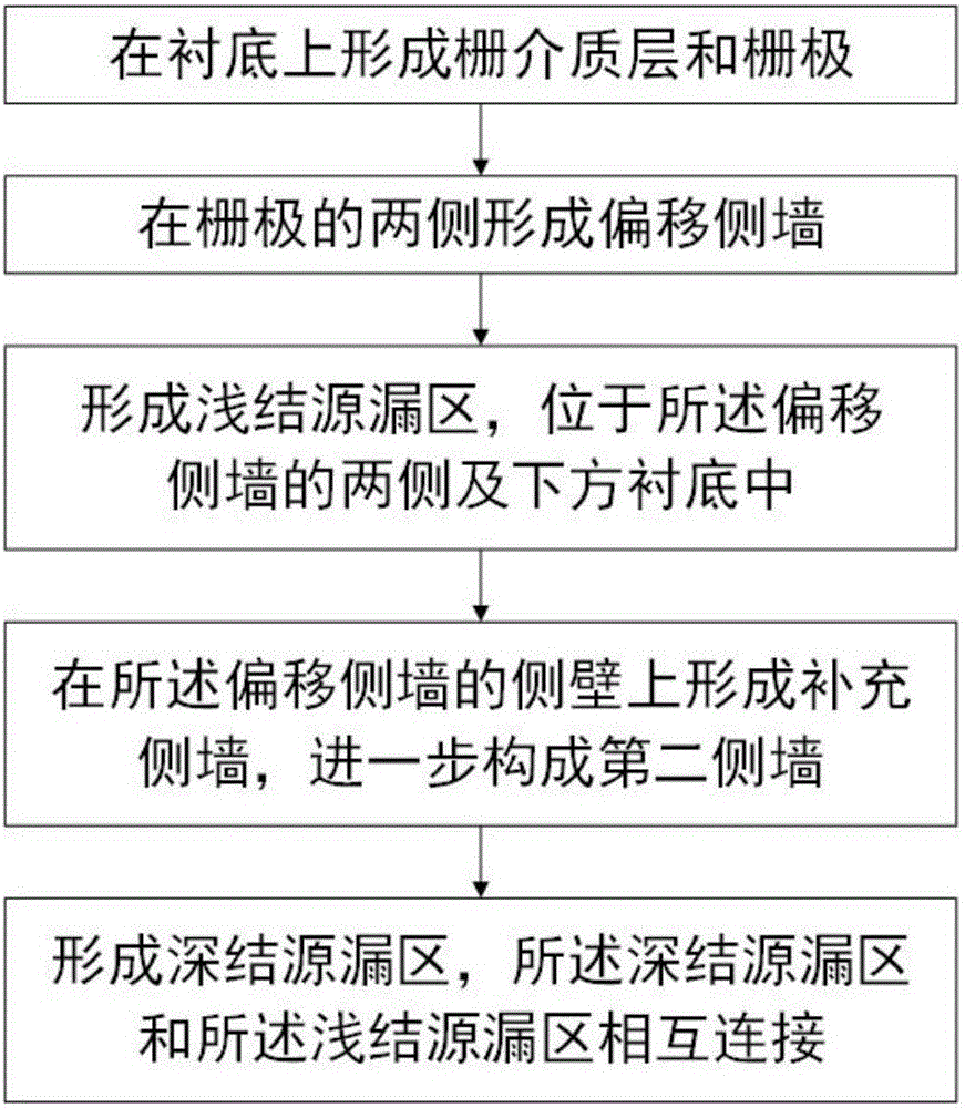
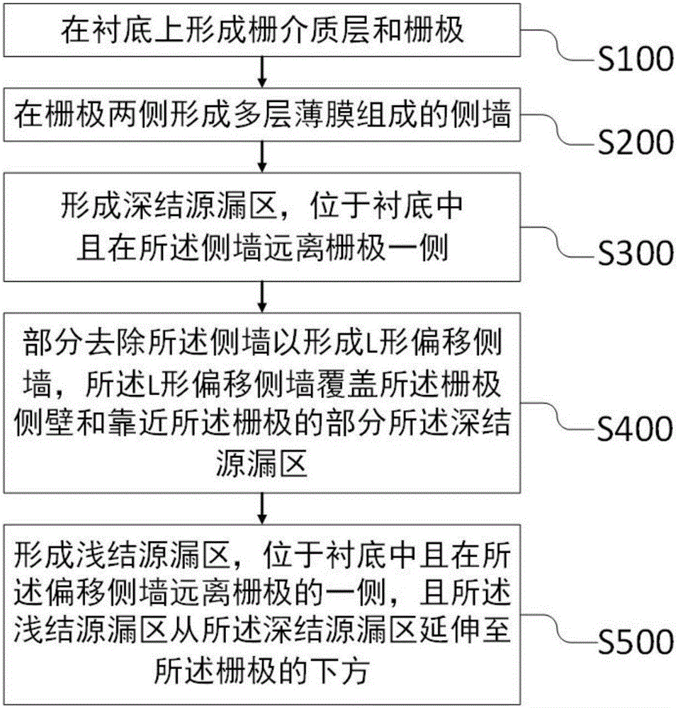
[0048] figure 2 It is a schematic flow diagram of the method for preparing a field effect transistor in Embodiment 1 of the present invention; Figure 3 to Figure 6 It is a structural schematic diagram of the method for manufacturing a field effect transistor in Embodiment 1 of the present invention during its preparation. The following reference figure 2 , image 3 , Figure 4 and Figure 5 , a specific embodiment of the present invention in detail, in this embodiment, the preparation method of the field effect transistor includes the following steps in sequence:

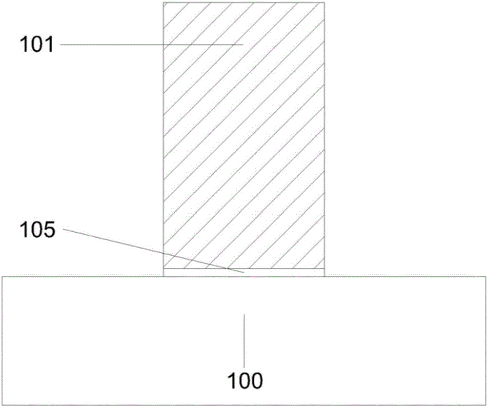
[0049] First, execute step S100, for details, refer to image 3As shown, a gate dielectric layer 105 and a gate 101 are formed on a substrate 100 , the gate 101 is formed on the gate dielectric layer 105 , and the substrate surface is exposed on both sides of the gate 101 . Optionally, the substrate 100 is a silicon substrate or a silicon germanium substrate, etc., the gate dielectric layer 105 is, for exam...

Embodiment 2

[0068] Figure 7 It is a schematic diagram of a partial structure during the preparation process of the field effect transistor preparation method in Example 2 of the present invention. combine Figure 5 and Figure 7 As shown, the difference from Embodiment 1 is that in this embodiment, the side wall adopts a two-layer structure. Therefore, the difference between the first embodiment and the second embodiment is mainly reflected in step S200 and step S400, therefore, only these two steps in this embodiment will be described in detail below.

[0069] Concrete combination figure 2 and Figure 7 As shown, in step S200 , during the process of forming sidewalls on both sides of the gate 101 , the structure of the formed sidewalls is a double-layer ON structure of silicon oxide layer 202 / silicon nitride layer 203 . The specific formation method can refer to the following steps: first, the silicon oxide layer 202 can be deposited by atomic layer deposition (Atomic Layer Depos...

Embodiment 3

[0072] Figure 8 It is a schematic diagram of the partial structure of the method for preparing the field effect transistor in the third embodiment of the present invention during its preparation process. combine Figure 7 and Figure 8 As shown, the difference from the second embodiment is that in this embodiment, the film layer in the sidewall close to the gate is a silicon oxide layer.

[0073] In this example, specific reference Figure 8As shown, in the step S200 , during the process of forming sidewalls on both sides of the gate 101 , the structure of the formed sidewalls is a double-layer NO structure of silicon nitride layer 302 / silicon oxide layer 303 . The specific formation method can refer to the following steps: first, the silicon nitride layer 302 can be deposited by atomic layer deposition (Atomic Layer Deposition, ALD) technology; then, silicon oxide can be deposited by chemical vapor deposition (Chemical Vapor Deposition, CVD) Layer 303, for example, the ...


PUM


Abstract

The invention relates to a field effect transistor and a forming method therefor. The method comprises the steps: firstly forming a side wall formed by multiple films, forming source and drain regions of a deep junction through the auto-collimation of the side wall, removing a part of the side wall to form an L-shaped deflecting side wall, and forming the source and drain regions of a shallow junction through the auto-collimation of the L-shaped deflecting side wall. According to the invention, the ion activation temperature of the source-drain regions of the deep and shallow junctions descends, and the L-shaped deflecting side wall is employed, so the method can achieve the effective control of the depth, concentration and contour of the shallow junction formed through the ion implantation of the source-drain region of the shallow junction. The device structure of the field effect transistor provided by the invention enlarges a technological window in a subsequent contact hole technological process. Meanwhile, the distance between a stress film and a device trench in the stress memory technology is reduced, and the carrier mobility is further improved, thereby improving the performances of a device.

Description

technical field [0001] The invention relates to the technical field of semiconductors, in particular to a field effect transistor and a forming method thereof. Background technique [0002] Field effect transistor fabrication technology is the foundation of the modern very large scale integration (VLSI) semiconductor industry. The market demand for high speed, high efficiency, and low energy consumption drives the semiconductor industry to develop continuously along Moore's Law. In order to meet market demand for high speed, high efficiency, and low energy consumption, semiconductor device units, especially Metal-Oxide-Semiconductor Field Effect transistors (MOSFETs), continue to shrink and enter the nanometer era. The shrinking of the device size requires the corresponding shrinking of the gate according to certain design rules, and in order to reduce the short channel effect, the junction depth of the source and drain should be reduced accordingly. [0003] figure 1 A p...

Claims


Application Information

Patent Timeline
IPC IPC(8): H01L21/336H01L29/78
Inventor 李翔刘哲宏
Owner SHANGHAI HUALI MICROELECTRONICS CORP
Why Eureka
Try Eureka