Forming method of semiconductor device

A semiconductor and device technology, applied in the field of semiconductor device formation, can solve problems such as increasing the difficulty of process control, reducing production efficiency, and increasing the probability of open circuits

Active Publication Date: 2020-04-17
SHANGHAI HUALI MICROELECTRONICS CORP
View PDF9 Cites 0 Cited by
  • Summary
  • Abstract
  • Description
  • Claims
  • Application Information

AI Technical Summary

Problems solved by technology

However, if figure 1 As shown, it is a schematic diagram of the thickness of the edge region of a wafer after chemical mechanical polishing. It can be seen that although this control process can make the edge region (the area > 146 mm from the center of the wafer) be chemically mechanically polished Reduced (still greater than the degree to which the wafer center area is ground), but the area other than the wafer edge area (that is, the area located inside the wafer edge area) in the wafer edge area (area > 142 mm from the wafer center), i.e. 142mm-146mm from the center of the wafer) is also less ground, resulting in a higher height than the center of the wafer (area < 142mm from the center of the wafer), resulting in a convex shape at the edge of the wafer. appearance
In the wafer edge region, the height of the region inside the crystal edge region is higher, which will increase the open window of the metal layer, so that the probability of opening the metal layer above the interlayer dielectric layer will increase, and the open window will increase to To a certain extent, the deposition and chemical mechanical polishing processes need to be re-performed, so that the open circuit window and short circuit window are controlled within a reasonable range, which reduces production efficiency and increases the difficulty of process control

Method used


Image

  • Forming method of semiconductor device
  • Forming method of semiconductor device
  • Forming method of semiconductor device

Examples


Embodiment Construction

[0026] The specific implementation manner of the present invention will be described in more detail below with reference to schematic diagrams. The advantages and features of the present invention will be more apparent from the following description. It should be noted that all the drawings are in a very simplified form and use imprecise scales, and are only used to facilitate and clearly assist the purpose of illustrating the embodiments of the present invention.

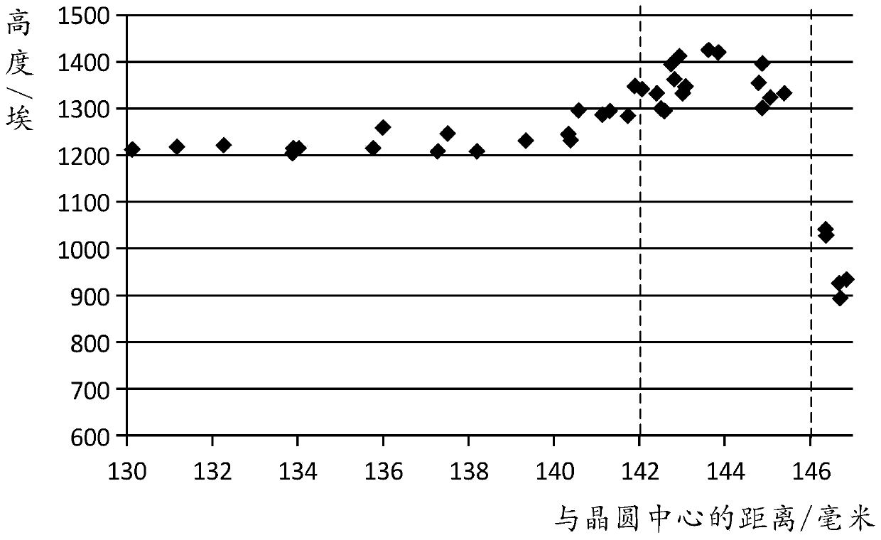
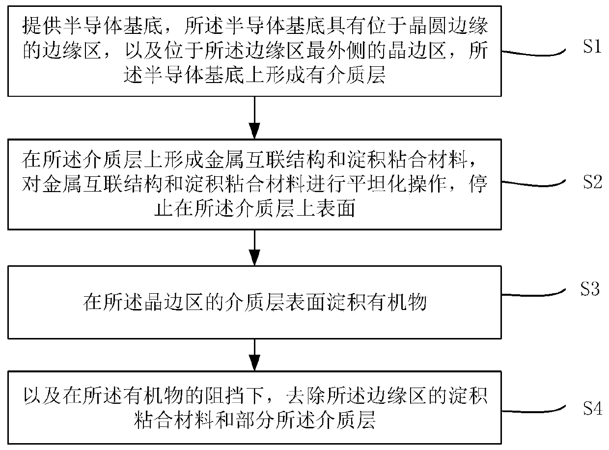
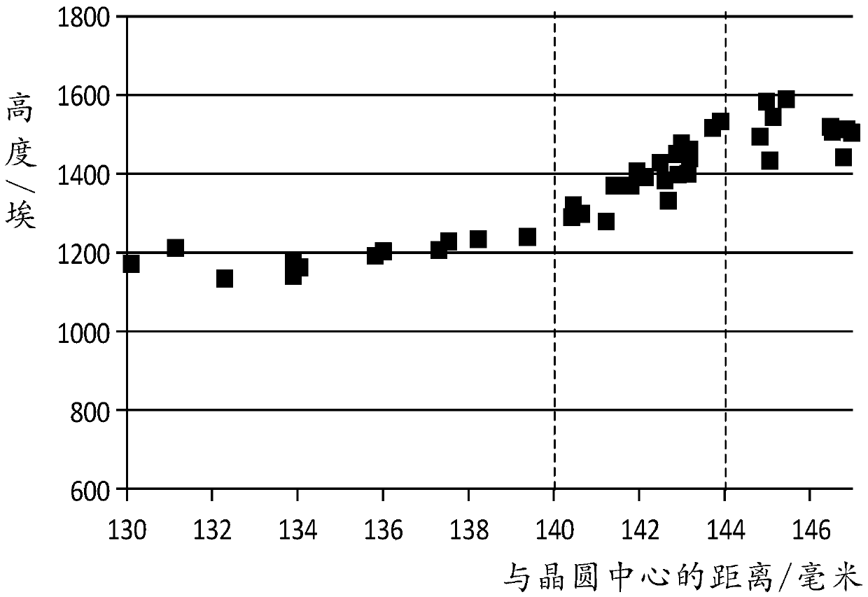
[0027] In order to increase the uniformity of film thickness in the edge region of the interlayer dielectric layer, the invention provides a method for forming a semiconductor device. figure 2 A process flow chart of a method for forming a semiconductor device provided by an embodiment of the present invention. Such as figure 2 As shown, the method for forming a semiconductor device according to the embodiment of the present invention includes the following steps:

[0028] Step S1: providing a semiconductor su...


PUM


Abstract

The invention provides a forming method of a semiconductor device. The forming method of the semiconductor device comprises the steps: providing a semiconductor substrate which is provided with an edge region located at the edge of a wafer and a wafer edge region located at the outermost side of the edge region, and forming a dielectric layer on the semiconductor substrate; forming a metal interconnection structure and a deposition bonding material on the dielectric layer, performing planarization operation on the metal interconnection structure and the deposition bonding material, and stopping on the upper surface of the dielectric layer; depositing an organic matter on the surface of the dielectric layer in the wafer edge region; and removing the deposition bonding material and part of the dielectric layer in the edge region under the blocking of the organic matter. According to the forming method of the semiconductor device, the protruding part of the dielectric layer in the wafer edge region can be selectively removed so that the uniformity of the thickness of the dielectric layer in the wafer edge region is improved, the process window is improved, and the rework frequency isreduced.

Description

technical field [0001] The invention relates to the field of semiconductor manufacturing, in particular to a method for forming a semiconductor device. Background technique [0002] With the development of semiconductor technology, the size of semiconductor devices continues to shrink, the corresponding technology nodes continue to improve, and the corresponding wafer bevel has an increasing influence on the manufacturing process. After processes such as chemical vapor deposition (Chemical Vapor Deposition, CVD), physical chemical vapor deposition (Physical Vapor Deposition, PVD), furnace tube process (furnace), photolithography and etching (etch) and other processes, it is located at the crystal edge The surface of the film (film) structure on the surface will become very rough. For example, in the process of forming the metal interconnection structure (Contact), it is necessary to deposit the glue layer (Glue layer) before the metal (such as tungsten) is deposited, so that...

Claims


Application Information

Patent Timeline
IPC IPC(8): H01L21/768H01L21/66
CPCH01L21/76838H01L21/76841H01L21/76819H01L22/26
Inventor 朱轶铮陆连
Owner SHANGHAI HUALI MICROELECTRONICS CORP
Why Eureka
Try Eureka