Substrate warping-resistant flip LED chip and preparation method thereof

An LED chip and warpage technology, applied in the field of flip-chip LED chips and their preparation, can solve problems such as poor voltage, dead lamp, chip damage, etc., to reduce package warpage, increase process window, and improve welding yield Effect

Pending Publication Date: 2021-01-15
FOSHAN NATIONSTAR SEMICON
View PDF0 Cites 1 Cited by
  • Summary
  • Abstract
  • Description
  • Claims
  • Application Information

AI Technical Summary

Problems solved by technology

[0003] Flip-chip LED chips have high requirements for the flatness of the packaging substrate. If the substrate is not flat, the chip is easy to be damaged (see figure 1 , the passivation layer cracks due to substrate warping and high stress); at the same time, substrate warping will also cause leakage, poor voltage and other defects, making the LED chip abnormally defective. According to statistics, when using a common substrate, the existing abnormal The defect rate (VF<5.8V) can reach more than 15%, even 65%; in addition, substrate warping can easily cause low soldering yield, leakage, and dead lights

Method used


Image

  • Substrate warping-resistant flip LED chip and preparation method thereof
  • Substrate warping-resistant flip LED chip and preparation method thereof
  • Substrate warping-resistant flip LED chip and preparation method thereof

Examples


Embodiment Construction

[0035] In order to make the object, technical solution and advantages of the present invention clearer, the present invention will be further described in detail below in conjunction with the accompanying drawings. It is only stated here that the words for directions such as up, down, left, right, front, back, inside, and outside that appear or will appear in the text of the present invention are only based on the accompanying drawings of the present invention, and are not specific to the present invention. limited.

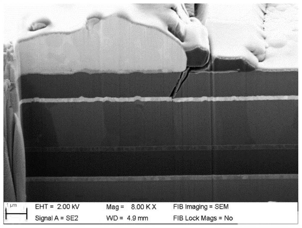
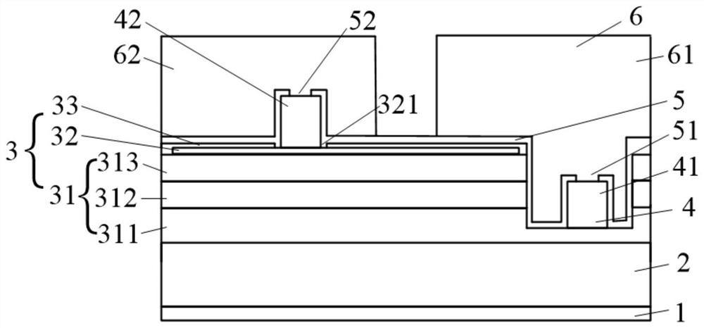
[0036] see figure 2 , the present invention provides a flip-chip LED chip resistant to substrate warpage, which includes a stress buffer layer 1, a substrate 2, a light emitting structure 3, a primary electrode structure 4, a passivation layer 5 and a secondary electrode structure 6; wherein, the stress The buffer layer 1 is disposed on the back side of the substrate 2, which can provide a stress opposite to the package stress direction, so as to relieve the wa...


PUM

PropertyMeasurementUnit
thicknessaaaaaaaaaa
thicknessaaaaaaaaaa
thicknessaaaaaaaaaa

Abstract

The invention discloses a substrate warping-resistant flip LED chip. The flip LED chip comprises a stress buffer layer, a substrate, a light-emitting structure, a primary electrode structure, a passivation layer and a secondary electrode structure. The light-emitting structure is arranged on the front surface of the substrate, the primary electrode structure is arranged on the light-emitting structure, the passivation layer is arranged on the primary electrode structure, and the secondary electrode structure is arranged on the passivation layer; the secondary electrode structure penetrates through the passivation layer and is connected with the primary electrode structure; the stress buffer layer is arranged on the back surface of the substrate. According to the invention, the stress buffer layer can provide the stress opposite to the packaging stress direction, thereby effectively reducing the packaging warping, enabling the flatness of the packaging substrate to be high, improving the welding yield, and improving the overall yield of the flip LED chip.

Description

technical field [0001] The invention relates to the technical field of optoelectronic manufacturing, in particular to a substrate warp-resistant flip-chip LED chip and a preparation method thereof. Background technique [0002] Flip-chip LED chip is a new type of LED chip. Its heat dissipation performance and light efficiency are better than ordinary LED chips, so it is widely used in various lighting products. Low-end applications such as bulb lamps and ceiling lamps, high-end applications such as car lights , street lamps, etc. . The packaging of flip-chip LED chips is quite different from that of traditional formal LED chips. Effective packaging is the key to the industrialization of flip-chip LED chips. [0003] Flip-chip LED chips have high requirements for the flatness of the packaging substrate. If the substrate is not flat, the chip is easy to be damaged (see figure 1 , the passivation layer cracks due to substrate warping and high stress); at the same time, subst...

Claims


Application Information

Patent Timeline
Patent Type & Authority Applications(China)
IPC IPC(8): H01L33/44H01L33/36H01L33/00
CPCH01L33/005H01L33/36H01L33/44H01L2933/0016H01L2933/0025
Inventor 仇美懿李进
Owner FOSHAN NATIONSTAR SEMICON
Why Eureka
Try Eureka