Memory and method of forming the same

A technology of memory and predetermined direction, which is applied in the manufacture of semiconductor devices, electrical solid-state devices, semiconductor/solid-state devices, etc. It can solve the problems of increased risk of short circuit, residual active area, and very large limitation of photolithography process window. Achieve the effect of reducing the risk of short circuit, simplifying the process and increasing the process window

Active Publication Date: 2022-07-19
FUJIAN JINHUA INTEGRATED CIRCUIT CO LTD
View PDF7 Cites 0 Cited by
  • Summary
  • Abstract
  • Description
  • Claims
  • Application Information

AI Technical Summary

Problems solved by technology

However, when the above method is used to form the bit line structure, due to the problem of alignment accuracy in the photolithography process, the problem of position shift or CD change will inevitably occur, so that the defined bit line trench d2 The location of the deviation (such as Figure 1b As shown, there is a leftward position deviation between the center line of the bit line trench d2 and the symmetry axis of the adjacent word line structure WL'), resulting in the formation of the bit line structure BL' in the bit line trench d2 and the After the node contact structure SC' is formed in the node contact window d1, the risk of a short circuit between the part of the bit line structure BL' protruding into the active area AA' and its adjacent node contact structure SC' increases, which will affect memory performance adversely affected
Moreover, as the device size shrinks, the lateral dimension between adjacent word line structures WL' is further shortened. In order to increase the bit line structure BL', the bit line structure BL' is usually extended laterally to the word line structure WL' When the bit line trench d2 deviates, the position of the part of the bit line structure BL' protruding into the active area AA' will shift and may cause the active area AA' to The remaining gg' in the active region caused by incomplete etching will further increase the risk of a short circuit between the bit line structure BL' and the nearby node contact structure SC', resulting in a very large limitation on the process window of the photolithography process

Method used


Image

  • Memory and method of forming the same
  • Memory and method of forming the same
  • Memory and method of forming the same

Examples


Embodiment 1

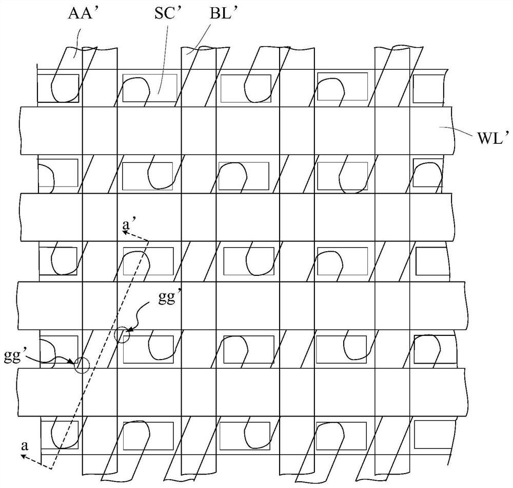
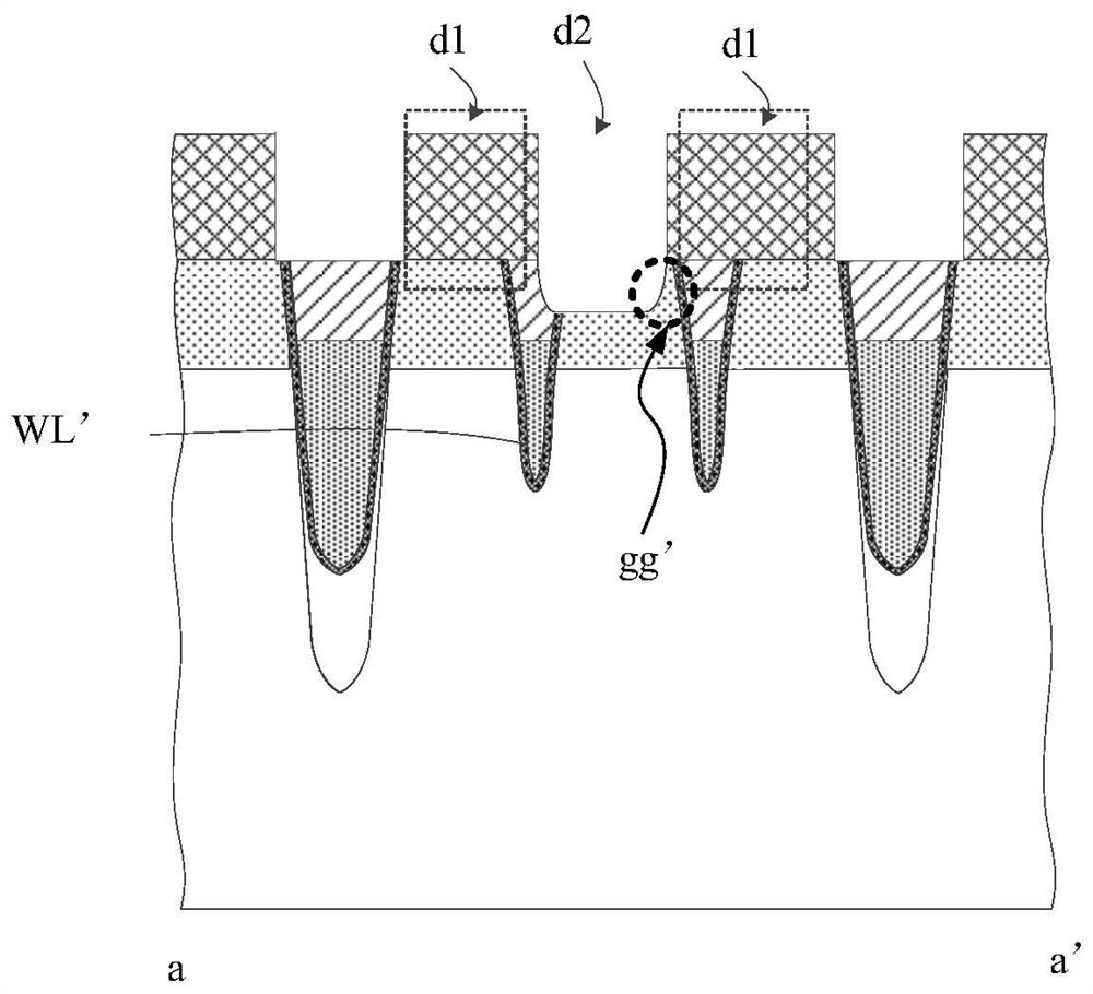
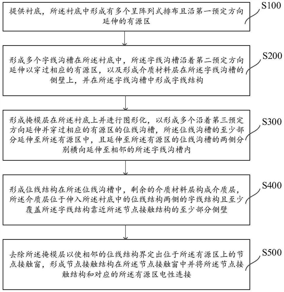
[0064] Figure 4f A schematic diagram of a partial structure of the memory in the first embodiment of the present invention, Figure 4g for Figure 4f Simplified layout of the memory in the Figure 4f for Figure 4g Schematic cross-sectional view of the memory in the a-a' direction. like Figure 4f as well as Figure 4g As shown, the memory includes: a substrate 100 and a word line structure WL formed in the substrate 100 .

[0065] A plurality of active regions AA and trench isolation structures STI are formed in the substrate 100 extending along a first predetermined direction (Z direction), and the trench isolation structures STI separate adjacent active regions AA. A plurality of the active areas AA are arranged in an array, and the active areas AA are independent of each other through the trench isolation structure STI, so as to avoid mutual interference between the active areas AA.

[0066] Further, word line trenches are also formed in the substrate 100, and the ...

Embodiment 2

[0142] Figure 5a It is a schematic diagram of a partial structure of the memory in the second embodiment of the present invention, Figure 5b for Figure 5a Simplified layout of the memory in the Figure 5a for Figure 5b Schematic cross-sectional view of the memory in the a-a' direction. like Figure 5a as well as Figure 5b As shown, the difference from the first embodiment is that in this embodiment, the dielectric layer only covers at least part of the sidewall of the second word line structure WL2 close to the node contact structure SC. That is to say, the dielectric layer only includes the first sidewall SP1.

[0143] Specifically, as Figure 5a As shown, the first spacer SP1 extends from the bottom of the node contact structure SC to a third depth position H3 ′ in the substrate 100 , that is, the top of the first spacer SP1 is located at the first At the depth position H1', ​​the first sidewall spacer SP1 extends from the first depth position H1' along the firs...


PUM


Abstract

The present invention provides a memory and a method for forming the same, comprising a substrate, a plurality of word line structures, a plurality of bit line structures, a plurality of node contact structures and a dielectric layer, wherein the dielectric layer is located in the word line structure in the active region, And at least cover at least part of the sidewall of the word line structure close to the node contact structure, so there is a dielectric layer isolation between the bit line structure and the node contact structure, reducing the part of the bit line structure extending into the active area and The risk of short circuit between the node contact structures improves the performance of the memory. Even if the position of the bit line trench is shifted, the bit line structure and the node contact structure can increase the isolation effect through the dielectric layer and increase the process window of the lithography process; And the dielectric layer is formed in the word line trench and before the word line structure. Since the outermost dielectric needs to be formed first when the word line structure is formed, the dielectric layer and the outermost dielectric of the word line structure can be in the same machine. Taichung has been formed successively, the process is simple and the cost is low.

Description

technical field [0001] The present invention relates to the field of semiconductor technology, and in particular, to a memory and a method for forming the same. Background technique [0002] A memory, such as a dynamic random access memory (DRAM), usually has a memory cell array, and the memory cell array includes a plurality of memory cells arranged in an array. The memory also has a plurality of bit line structures, each of which is electrically connected to a corresponding storage unit, and the memory further includes a storage capacitor for storing charges representing stored information, and the storage capacitors. The storage unit can be electrically connected to the storage capacitor through a node contact structure, so as to realize the storage function of each storage unit. [0003] Figure 1a is a simplified layout of an existing memory, Figure 1b for Figure 1a A schematic cross-sectional view of the memory in the a-a' direction. combine Figure 1a and Figur...

Claims


Application Information

Patent Timeline
Patent Type & Authority Patents(China)
IPC IPC(8): H01L27/108H01L21/8242
CPCH10B12/34H10B12/315H10B12/482H10B12/488H10B12/485
Inventor 冯立伟
Owner FUJIAN JINHUA INTEGRATED CIRCUIT CO LTD
Why Eureka
Try Eureka