Level shift circuit and driver circuit using the same

a technology of driver circuit and level shift circuit, which is applied in logic circuits, pulse automatic control, pulse techniques, etc., can solve problems such as the possibility of error operation, and achieve the effect of avoiding output delay and error operations, high speed and reliability, and operating reliably at high speed

Inactive Publication Date: 2007-06-28
NEC CORP
View PDF7 Cites 16 Cited by
  • Summary
  • Abstract
  • Description
  • Claims
  • Application Information

AI Technical Summary

Benefits of technology

[0065] According to the present invention, a level shift circuit capable of operating reliably at high speed even with a small input signal amplitude, or a low signal voltage, and a large amplitude of a signal level-shifted and outputted is realized while avoiding output delay and error operations, and it is capable of meeting the demands for higher speed and reliability. Further, according to the present invention, the circuit is suitable for use as a driver of such a display device. Further, it becomes suitable for use in a receiver circuit by having the level shift circuit of the present invention in a stage following a differential circuit that differentially receives input signals.

Problems solved by technology

However, in a conventional level shift circuit, an error operation is likely to occur when the ratio of the input amplitude against the output amplitude is small.

Method used


Image

  • Level shift circuit and driver circuit using the same
  • Level shift circuit and driver circuit using the same
  • Level shift circuit and driver circuit using the same

Examples


Embodiment Construction

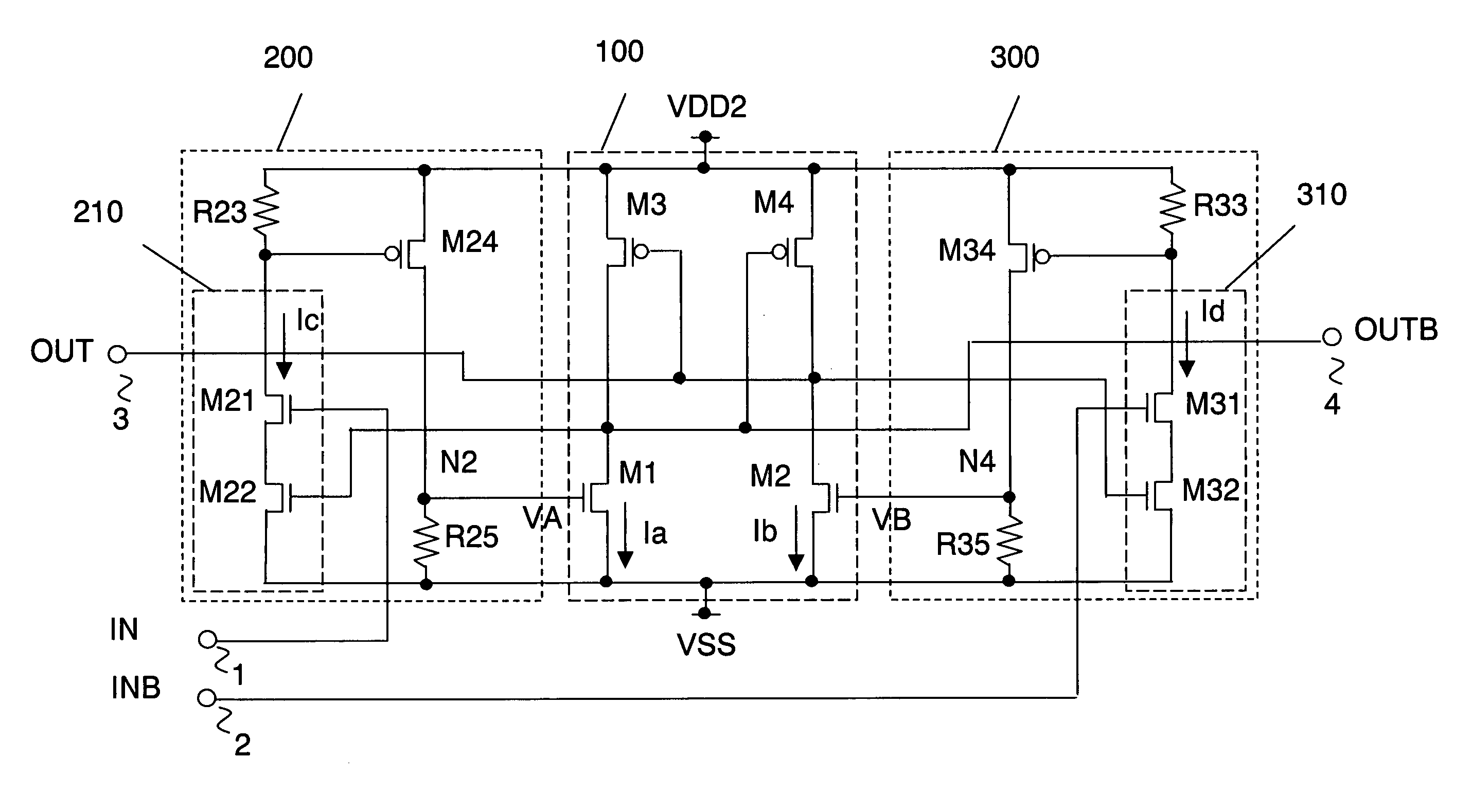
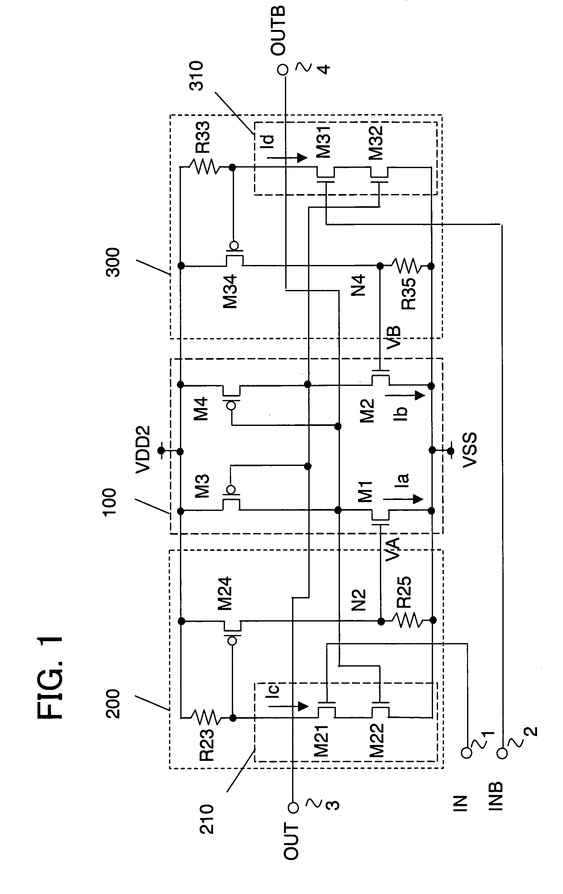
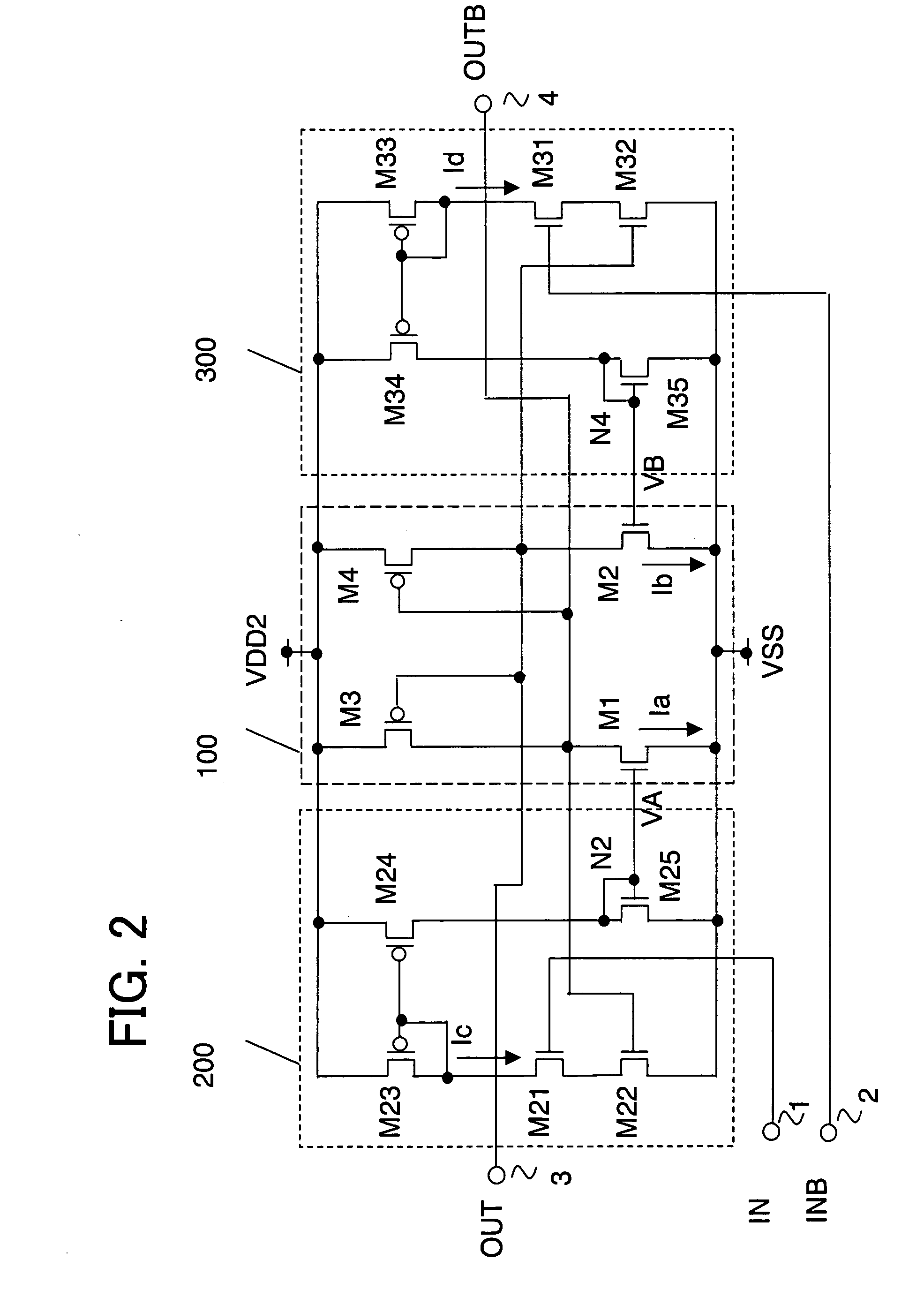
[0091] The various aspects and modes of the present invention will be further described in detail with reference to the attached drawings. A level shift circuit relating to a first example of the present invention comprises first and second terminals (1 and 2) that respectively receive an input signal (IN) and its complementary signal (INB) having a first amplitude, third and fourth terminals (3 and 4) that respectively output an output signal (OUT) and its complementary signal (OUTB) having a second amplitude, which is larger than the first amplitude, an output circuit (100) comprising first and second transistors (M1 and M2) of a first polarity respectively connected between a first power supply (VSS) and the fourth terminal and between the first power supply (VSS) and the third terminal, and third and fourth transistors (M3 and M4) of a second polarity, respectively connected between a second power supply (VDD2) and the first transistor (M1) and between the second power supply (V...


PUM


Abstract

A level shift circuit operates normally when amplitude of input signal is small and amplitude of output signal is large. First and second terminals receive an input signal and its complementary signal having a first amplitude. Third and fourth terminals output an output signal and its complementary signal having a second amplitude, which is larger than the first amplitude. Output circuit comprises first and second transistors of first polarity respectively connected between first power supply and fourth and third terminals, respectively. Third and fourth transistors of second polarity, respectively, are connected between second power supply and fourth and third terminals, respectively, having control ends connected to the third and the fourth terminals, respectively. First current control circuit controls so that a current driving the fourth terminal flows through the first transistor according to the input signal and the complementary signal of the output signal. Second current control circuit controls so that a current driving the third terminal flows through the second transistor according to the complementary signal of the input signal and the output signal.

Description

FIELD OF THE INVENTION [0001] The present invention relates to a level shift circuit and a driver circuit using the same. BACKGROUND OF THE INVENTION [0002] In recent years, liquid crystal displays (LCD), characterized by their thinness, light-weightiness, and low power consumption, have been widely used as display devices, and it has become possible to realize a large-screen LCD TV as technologies to enlarge screens and support moving pictures are improved. As the liquid crystal display device, active matrix LCD devices allowing high definition display are currently in use. First, referring to FIG. 21, a typical configuration of an active matrix LCD device will be described. Note that a main structure connected to a pixel of the liquid crystal display unit is schematically shown by an equivalent circuit diagram in FIG. 21. [0003] The display unit (a display panel) 960 of the active matrix LCD device is generally constituted by a semiconductor substrate on which transparent pixel el...

Claims


Application Information

Patent Timeline
Patent Type & Authority Applications(United States)
IPC IPC(8): H03L5/00
CPCH03K3/35613
Inventor TSUCHI, HIROSHIMIYASAKA, DAIGO
Owner NEC CORP
Why Eureka
Try Eureka