Interconnection of Semiconductor Device and Method for Manufacturing the Same

a technology of interconnection and semiconductor, which is applied in the direction of semiconductor/solid-state device manufacturing, basic electric elements, electric devices, etc., can solve the problems of low melting point and high specific resistance metals that are not suitable for high-integrated semiconductor devices, bad influence on device reliability, and degradation of device yield rate, etc., to improve the reliability of semiconductor devices

Inactive Publication Date: 2007-06-28
DONGBU ELECTRONICS CO LTD
View PDF2 Cites 16 Cited by
  • Summary
  • Abstract
  • Description
  • Claims
  • Application Information

AI Technical Summary

Benefits of technology

[0010] An object of the present invention is to provide an interconnection of a semiconductor device and a method for manufacturing the same, capable of improving reliability of a semiconductor device.

Problems solved by technology

However, as the semiconductor device has become highly integrated, such metals having a low melting point and a high specific resistance are not suitable for the highly integrated semiconductor device.
In this case, due to over-polish and the increase of CMP speed, scratch or a dishing phenomenon causing a surface of the conductive layer to be recessed may be generated.
The copper interconnection having dishing phenomenon or scratch may not be easily connected to a via of an upper copper metal, so that electricity is interrupted or resistance is increased, thereby exerting bad influence upon the reliability of the device.
Further, in the case of excessive scratch, the copper interconnection is not connected with the upper metal layer, thereby causing degradation of the device yielding rate.

Method used


Image

  • Interconnection of Semiconductor Device and Method for Manufacturing the Same
  • Interconnection of Semiconductor Device and Method for Manufacturing the Same
  • Interconnection of Semiconductor Device and Method for Manufacturing the Same

Examples


Embodiment Construction

[0017] Hereinafter, preferred embodiments of the present invention will be described in detail with reference to the accompanying drawings. However, the present invention is not limited to these embodiments, but various modifications and variations can be made within the scope of the present invention. Such modifications and variations are also within the scope of the appended claims.

[0018] In the figures, thickness of layers and areas will be enlarged for the purpose of clarity, and the same reference numerals will be used to refer to the same or like elements throughout the description. When layers, films, areas and plates are expressed as they are formed on other elements, it may not exclude another elements interposed therebetween. In contrast, if elements are expressed as they are directly formed on other elements, it may exclude other elements interposed therebetween.

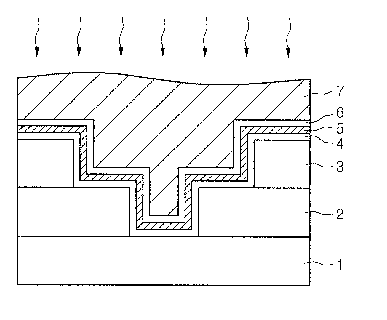
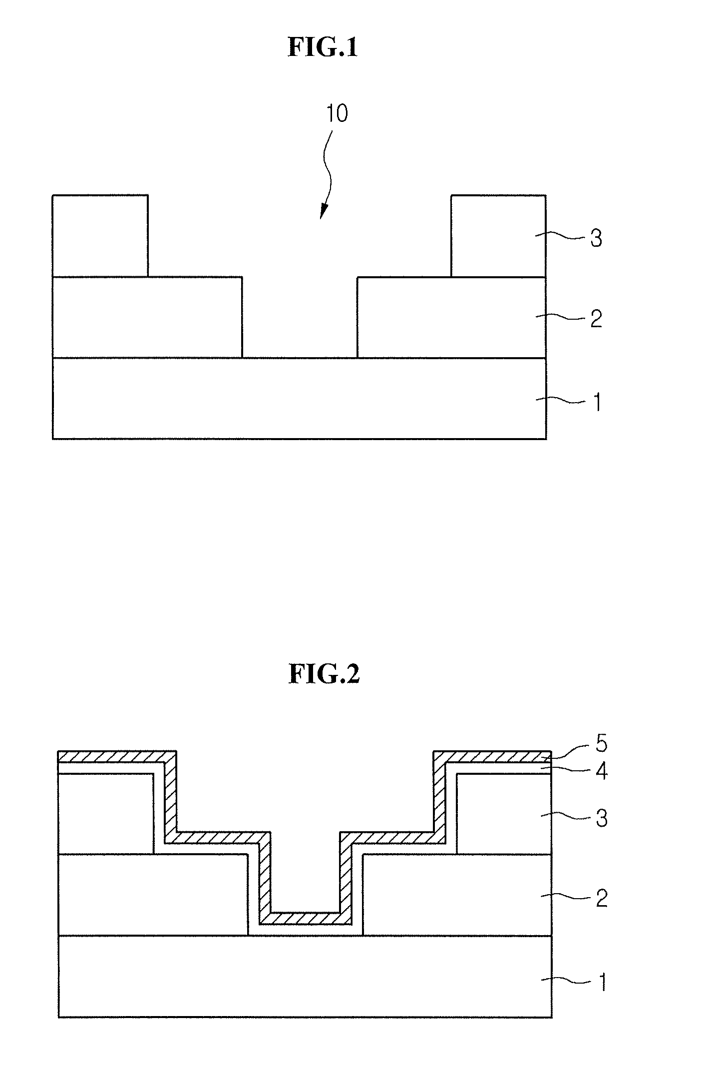
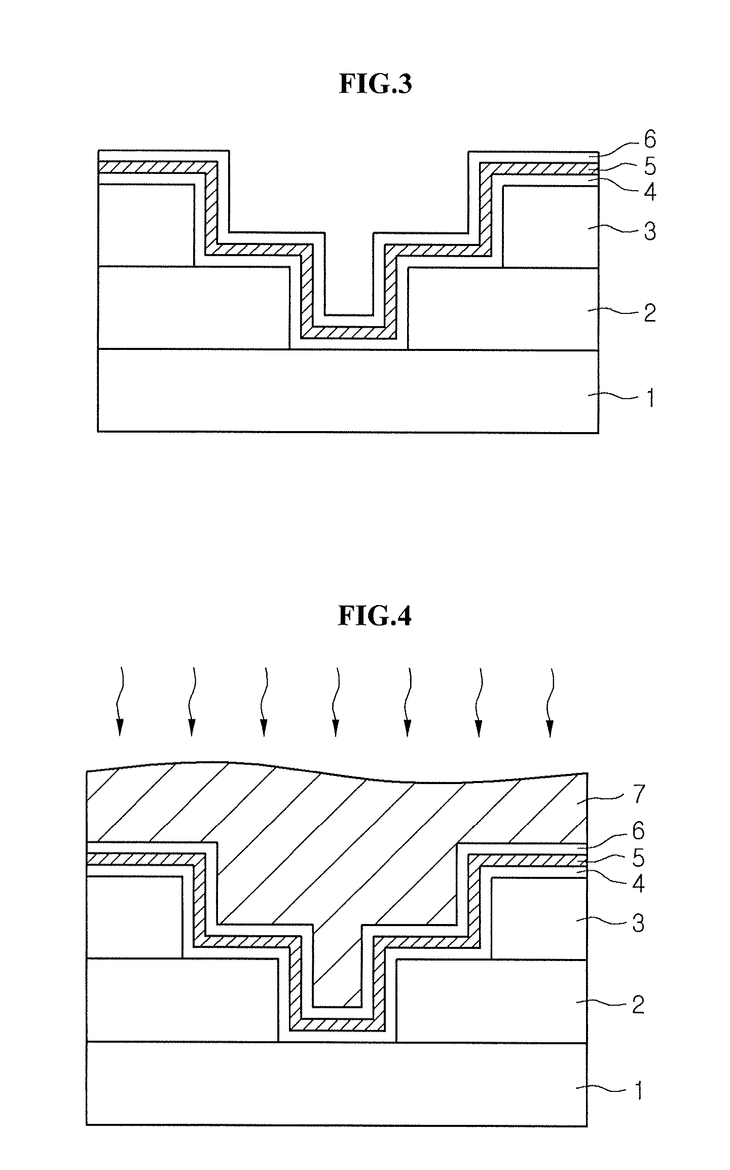
[0019] FIGS. 1 to 6 are views for illustrating a method for forming a damascene interconnection of a semicond...


PUM

PropertyMeasurementUnit
temperatureaaaaaaaaaa
thicknessaaaaaaaaaa
melting pointaaaaaaaaaa

Abstract

A method for manufacturing an interconnection of a semiconductor device is provided. The method can include the steps of: forming an interlayer dielectric layer on a semiconductor substrate; forming a damascene pattern on the interlayer dielectric layer; depositing a seed layer on the interlayer dielectric layer; depositing a metal layer on the seed layer; depositing a copper layer on the metal layer for forming a copper interconnection; and performing a heat treatment process such that the metal layer reacts with the copper layer to produce an alloy layer including copper.

Description

RELATED APPLICATION [0001] This application claims the benefit under 35 U.S.C. §119(e), of Korean Patent Application Number 10-2005-0131200 filed Dec. 28, 2005, which is incorporated herein by reference in its entirety. FIELD OF THE INVENTION [0002] The present invention relates to an interconnection of a semiconductor device and a method for manufacturing the same. BACKGROUND OF THE INVENTION [0003] In manufacturing a semiconductor device, a metal interconnection is used to electrically connect devices and interconnections to each other. Aluminum (Al), aluminum alloys and tungsten (W) have been extensively used as materials for the metal interconnection. [0004] However, as the semiconductor device has become highly integrated, such metals having a low melting point and a high specific resistance are not suitable for the highly integrated semiconductor device. [0005] The materials having superior conductivity such as copper (Cu), gold (Au), silver (Ag), cobalt (Co), chrome (Cr) or n...

Claims


Application Information

Patent Timeline
Patent Type & Authority Applications(United States)
IPC IPC(8): H01L21/44
CPCH01L21/7684H01L21/76843H01L21/76846H01L21/76847H01L21/76864H01L21/28
Inventor LEE, HAN CHOON
Owner DONGBU ELECTRONICS CO LTD
Why Eureka
Try Eureka