DC offset correction for high gain complex filter

a dc offset and complex filter technology, applied in the direction of amplitude demodulation, line-fault/interference reduction, pulse technique, etc., can solve the problem of dc-offset correction circuit rejecting very low frequencies, waveform to clip over a smaller range of signal amplitudes, and large resistance requirements

Active Publication Date: 2007-07-05
QUALCOMM INC
View PDF25 Cites 14 Cited by
  • Summary
  • Abstract
  • Description
  • Claims
  • Application Information

AI Technical Summary

Problems solved by technology

“The response at DC is not always critical, but excessive DC offset will alter the output waveform symmetry about zero volts; possibly causing the waveform to clip over a smaller range of signal amplitud

Method used


Image

  • DC offset correction for high gain complex filter
  • DC offset correction for high gain complex filter
  • DC offset correction for high gain complex filter

Examples


Embodiment Construction

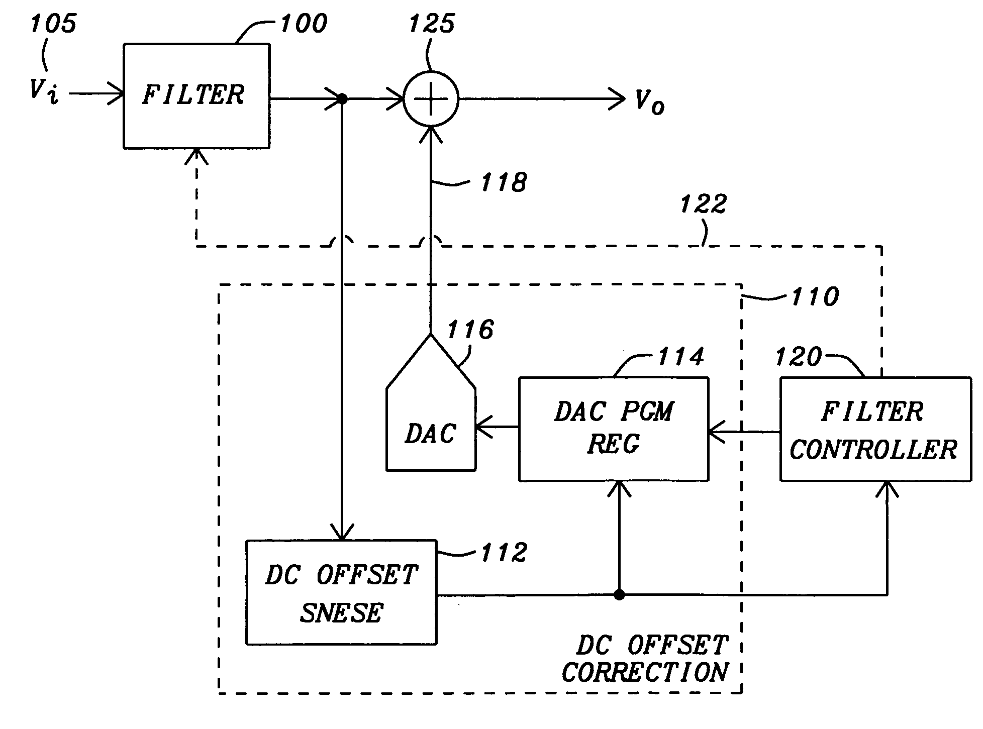
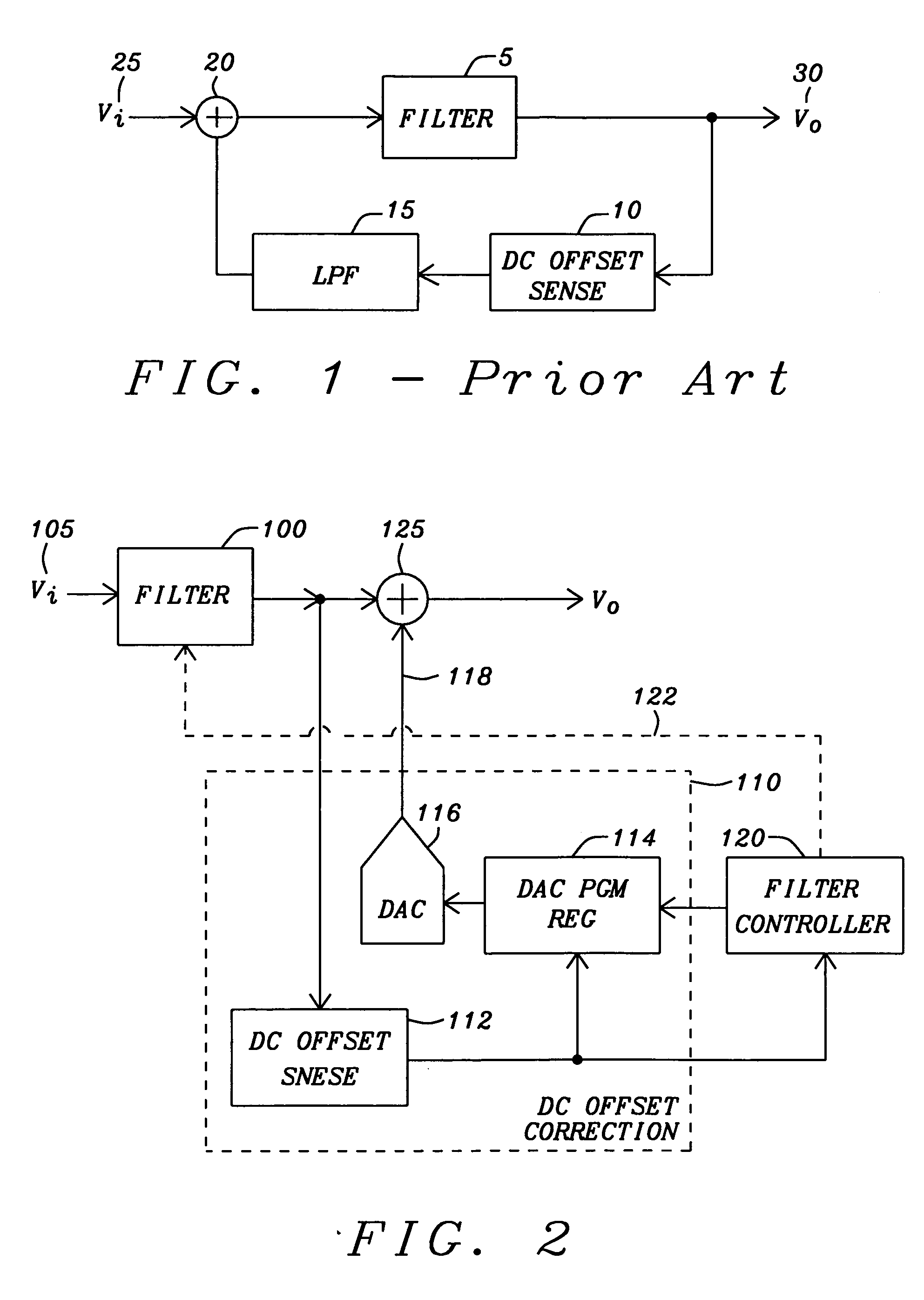
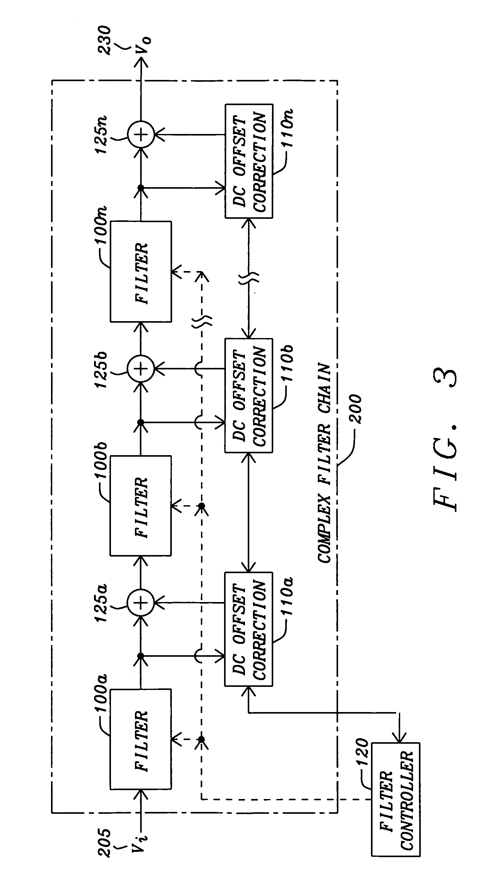
[0029] A DC voltage offset correction circuit of this invention provides for correction and compensation of a DC offset voltage of an output of a filter stage of a complex filter circuit and includes a DC offset sensing device and a digital-to-analog converter. The DC offset sensing device is connected to an output of a filter stage of a complex filter to generate an offset presence signal indicating presence of the DC offset voltage at the output of the filter stage. The digital-to-analog converter is in communication with the DC offset sensing device and connected to the output of the filter stage to apply a compensation signal to the output conditional on the offset presence signal.

[0030] A programming register is in communication with the DC offset sensing device to receive the offset presence signal. From the offset presence signal, the programming register performs a binary search to generate a digital signal indicative of a magnitude of the compensation signal. The programmi...


PUM


Abstract

A DC voltage offset correction circuit that provides for correction of a DC offset voltage of an output of a filter stage of a complex filter circuit includes a DC offset sensing device that is connected to an output of a filter stage of a complex filter to generate an offset presence signal indicating presence of the DC offset voltage at the output of the filter stage. The digital-to-analog converter applies a compensation signal to the output conditional on the offset presence signal. A programming register receives the offset presence signal to perform a binary search to generate a digital signal to force the digital-to-analog converter to apply the compensation voltage to the output of the filter stage. A filter controller sets the compensation voltage level in the programming register to match a programmed gain value of the filter stage.

Description

BACKGROUND OF THE INVENTION [0001] 1. Field of the Invention [0002] This invention relates to methods and apparatus for correcting DC offset voltage in electronic circuits. More particularly, this invention relates to correction of DC offset compensation device automatically eliminating a DC offset voltage at the output of gain stage of a complex filter. [0003] 2. Description of Related Art [0004] As is known in the art, the gain stages of a complex filter are operational amplifiers. It is further known in the art and explained in Design of Analog Integrated Circuits and Systems, Laker and Sansen, McGraw-Hill, New York, N.Y., January 1994, pp.: 448-450, “in an ideal op amp, if the input signal is zero, the output will also be zero. In an op amp, imperfections in the circuit components cause a DC voltage Vout to exist at the output, even when the input voltage is zero”. “The response at DC is not always critical, but excessive DC offset will alter the output waveform symmetry about z...

Claims


Application Information

Patent Timeline
IPC IPC(8): H03D1/04
CPCH03F3/45475H03F3/45968H03F2200/375H03H2011/0494H03F2203/45212H03F2203/45354H03H11/1291H03F2203/45138H03D1/04
Inventor GUPTA, RAVI
Owner QUALCOMM INC
Why Eureka
Try Eureka