Method of singulating a microelectronic wafer

a microelectronic and wafer technology, applied in the direction of basic electric elements, semiconductor/solid-state device manufacturing, electric apparatus, etc., can solve the problems of inapplicability of dbg method to wafers comprising low k materials, inability to work with dbg tools, and inability to meet the requirements of k material requirements,

Inactive Publication Date: 2007-07-05
INTEL CORP
View PDF15 Cites 69 Cited by
  • Summary
  • Abstract
  • Description
  • Claims
  • Application Information

AI Technical Summary

Problems solved by technology

Disadvantageously, the DBG method is not applicable to wafers comprising a low k material, such as wafers typically having a diameter of 300 mm or above, without substantial costly, complicated, and sometimes unreliable modifications to the DBG tools.
For example, for wafers including carbon doped oxides (i.e.: SiO2+C) which make the dielectric layers more brittle, the existing DBG method involving a sawing of a bare wafer is no longer workable, to the extent that the low k materials too brittle to allow a bare wafer saw process, and are susceptible to chipping, breakage and cracking as a result.
However, since wafers including low k materials are typically br...

Method used


Image

  • Method of singulating a microelectronic wafer
  • Method of singulating a microelectronic wafer
  • Method of singulating a microelectronic wafer

Examples


Embodiment Construction

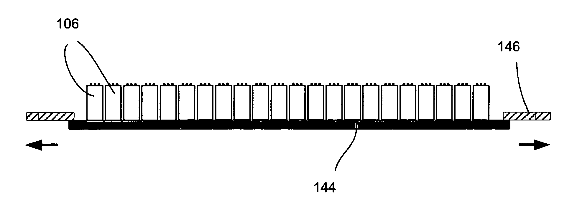
[0009] In the following detailed description, a method embodiment of singulating a wafer is disclosed. Reference is made to the accompanying drawings within which are shown, by way of illustration, specific embodiments by which the present invention may be practiced. It is to be understood that other embodiments may exist and that other changes may be made without departing from the scope and spirit of the present invention.

[0010] The terms on, above, below, and adjacent as used herein refer to the position of element relative to other elements. As such, a first element disposed on, above, or below a second element may be directly in contact with the second element or it may include one or more intervening elements. In addition, a first element disposed next to or adjacent a second element may be directly in contact with the second element or it may include one or more intervening elements.

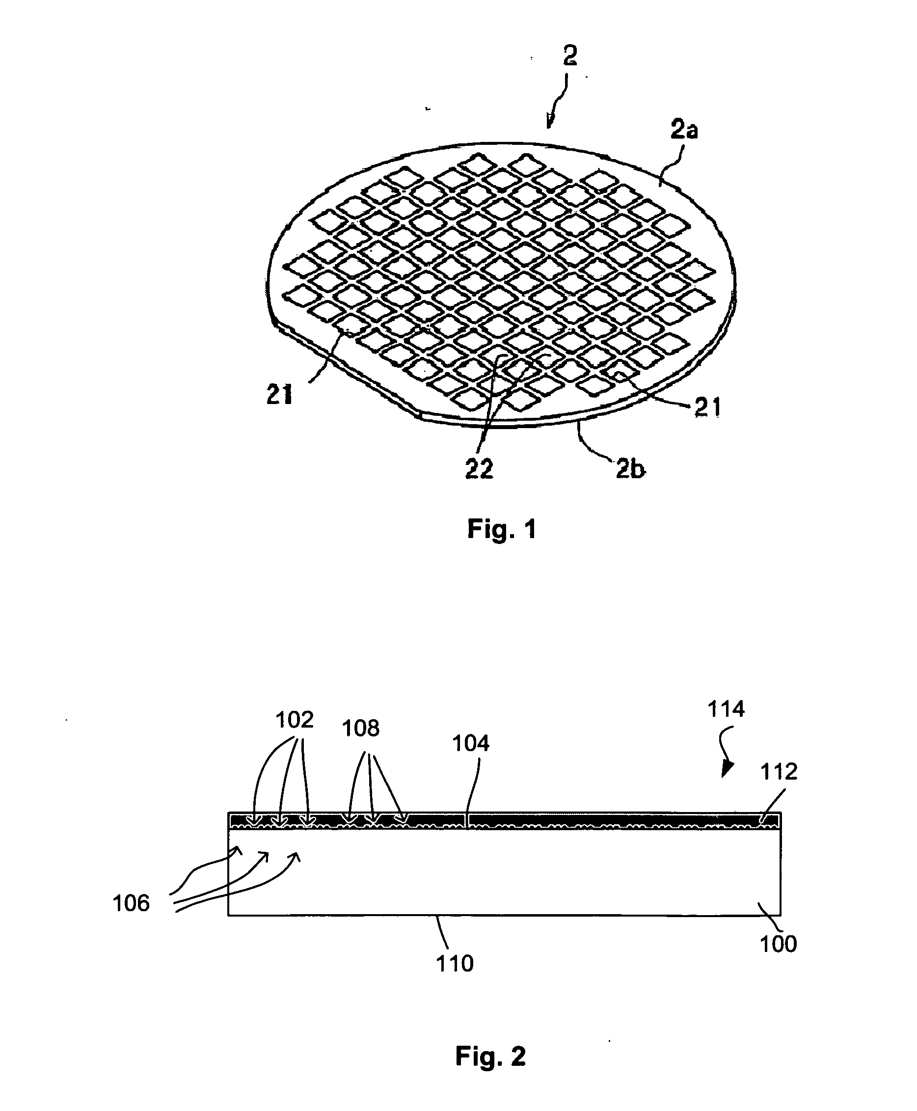
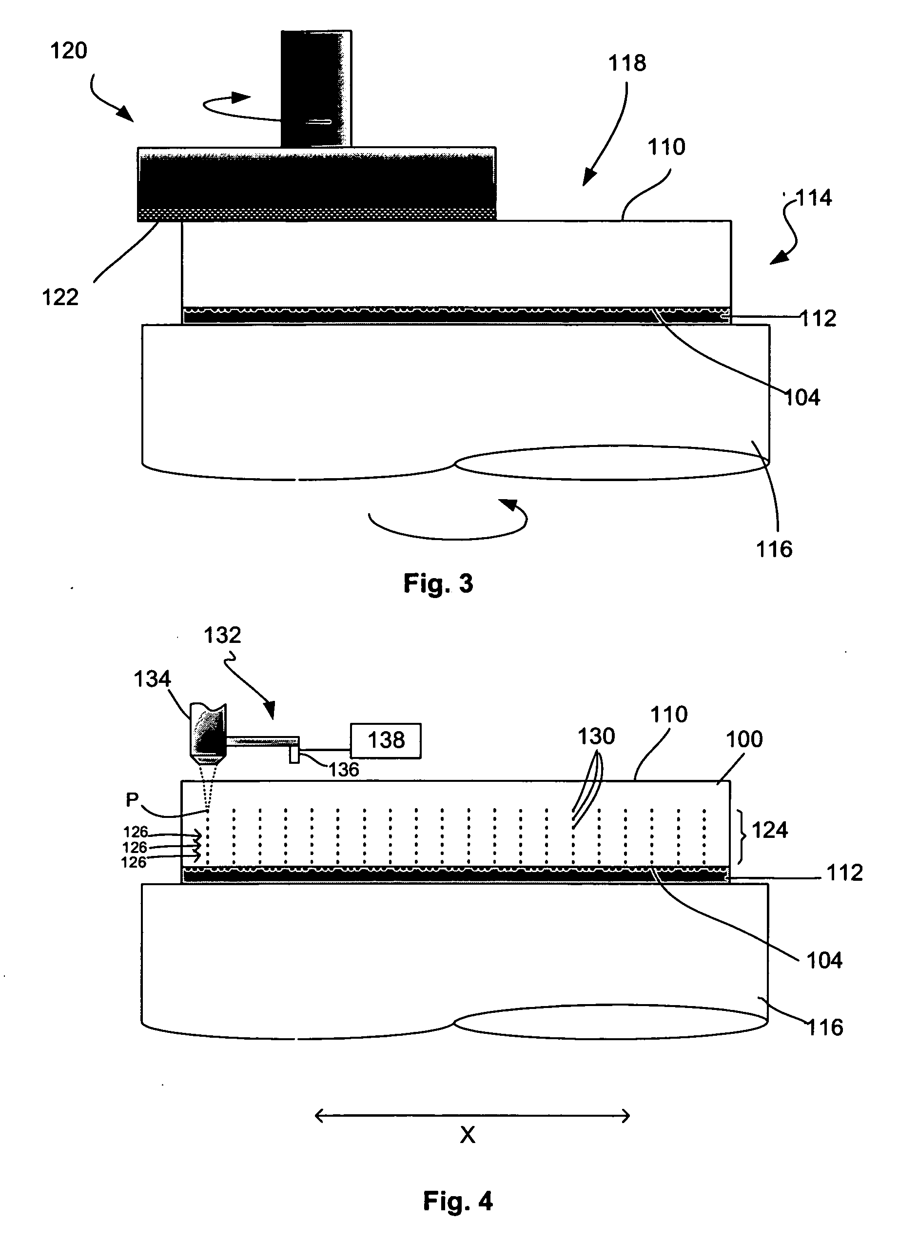
[0011] Referring first to FIG. 1, a perspective view of a conventional microelectronic wafer...


PUM


Abstract

A method of singulating a microelectronic wafer. The method comprises: providing a microelectronic wafer; focusing a laser beam in an interior region of the wafer from the backside of the wafer to form a modified region extending along the severance lines of the wafer dividing the wafer IC chips, the modified region further extending from an undersurface of the active surface and ending at a predetermined depth with respect to the backside. The modified region comprises a plurality of modified sites of the wafer molten by the laser and resolidified. The method further includes reducing a thickness of the wafer in a direction from the backside toward the active surface by a reduction amount equal to at least the predetermined depth; and dividing the wafer into individual IC chips along the severance lines at the modified sites.

Description

FIELD OF THE INVENTION [0001] Embodiments of the present invention relate to a method of singulating a wafer. BACKGROUND OF THE INVENTION [0002] Singulating microelectronic wafers, also known as dicing or die separation, is the process of cutting a microelectronic substrate having integrated circuit chips or “IC” chips formed thereon into individual microelectronic dice. Currently, although a number of methods for singulating microelectronic wafers are known, the most commonly used methods involve cutting the wafer along scribe or severance lines (commonly termed “streets”) on an active surface of the wafer with a rotating circular abrasive saw blade or dicer. [0003] One way to singulate microelectronic wafers is to use a method called dicing-before-grinding, or a dice before grind (DBG) method, typically used on 200 mm diameter wafers usually made of bulk silicon and a combination of copper and aluminum for the circuit layers. According to the DBG method, a microelectronic wafer is...

Claims


Application Information

Patent Timeline
IPC IPC(8): H01L21/30
CPCH01L21/78
Inventor CONTES, ANDREW N.
Owner INTEL CORP
Why Eureka
Try Eureka