Simultaneous display of eye diagram and jitter profile during device characterization

a technology of jitter profile and eye diagram, which is applied in the direction of electrical digital data processing, instruments, transmission, etc., can solve the problems of unbounded random jitter, difficult characterization, and difficulty in testing engineers, so as to facilitate random jitter measurement, easy identification of relationships, and the effect of improving the accuracy of the testing procedur

Inactive Publication Date: 2007-07-05
AVAGO TECH WIRELESS IP SINGAPORE PTE
View PDF3 Cites 24 Cited by
  • Summary
  • Abstract
  • Description
  • Claims
  • Application Information

AI Technical Summary

Benefits of technology

[0014] The present invention provides significant improvements over prior art devices because a user is able to more easily measure random jitter and observe eye diagrams. Furthermore, the user is able to more easily identify relationships between the random jitter measurements and eye diagrams. In one embodiment of the invention, a bit error rate tester (“BERT”), oscilloscope, one or more function generators and a jitter generator are used to test a particular electrical device. A control may be used to change the device settings based on both random jitter and eye opening observations.
[0015] Because the invention allows simultaneous observation of an eye diagram and jitter data, the electrical device being tested is not required to be connected and disconnected to and from various jitter measurement devices and oscilloscopes. The control attached to the device being tested may be used to modify device settings relative to real-time displays of random jitter and the eye diagram. Accordingly, the testing procedure becomes relatively more accurate and easier for a user to perform.

Problems solved by technology

In particular, the importance of properly measuring signal characteristics, such as a signal-to-noise ratio, jitter, and other signal integrity characteristics, may become even more important as communications systems become increasingly complex.
The task of efficiently measuring these different types of jitter, and optimizing the device accordingly, may present difficulties to a test engineer.
Comparatively, random jitter is unbounded and much more difficult to characterize.
Random jitter may be generated from various sources including thermal noise, shot noise, white noise, etc. and is relatively more difficult to predict.
Also, there may exist uncorrelated jitter on a signal, which is caused by non-synchronized noise generated by one or more different clocks within a system.
As explained above, the eye diagram does not allow efficient monitoring of random jitter component.
The eye diagram may be used to determine whether a transmitter, receiver or other device is compliant to a specification; however, it often fails to provide enough information or distinct values for accurate jitter measurements.
This makes the procedure of device characterization cumbersome and error prone since it requires repeatedly attaching and detaching the electrical device 102 to either the oscilloscope 104 or jitter measuring device 106.

Method used


Image

  • Simultaneous display of eye diagram and jitter profile during device characterization
  • Simultaneous display of eye diagram and jitter profile during device characterization
  • Simultaneous display of eye diagram and jitter profile during device characterization

Examples


Embodiment Construction

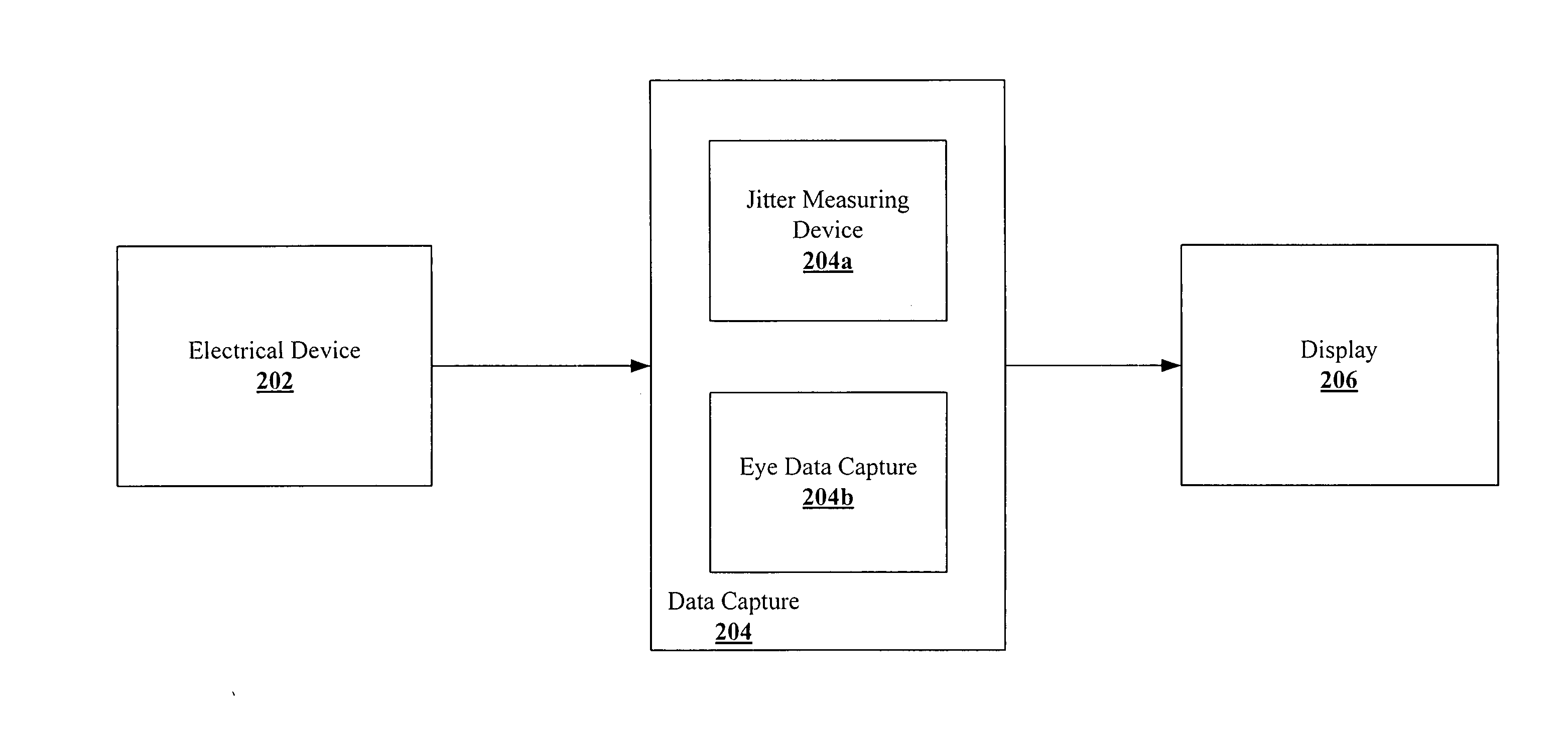
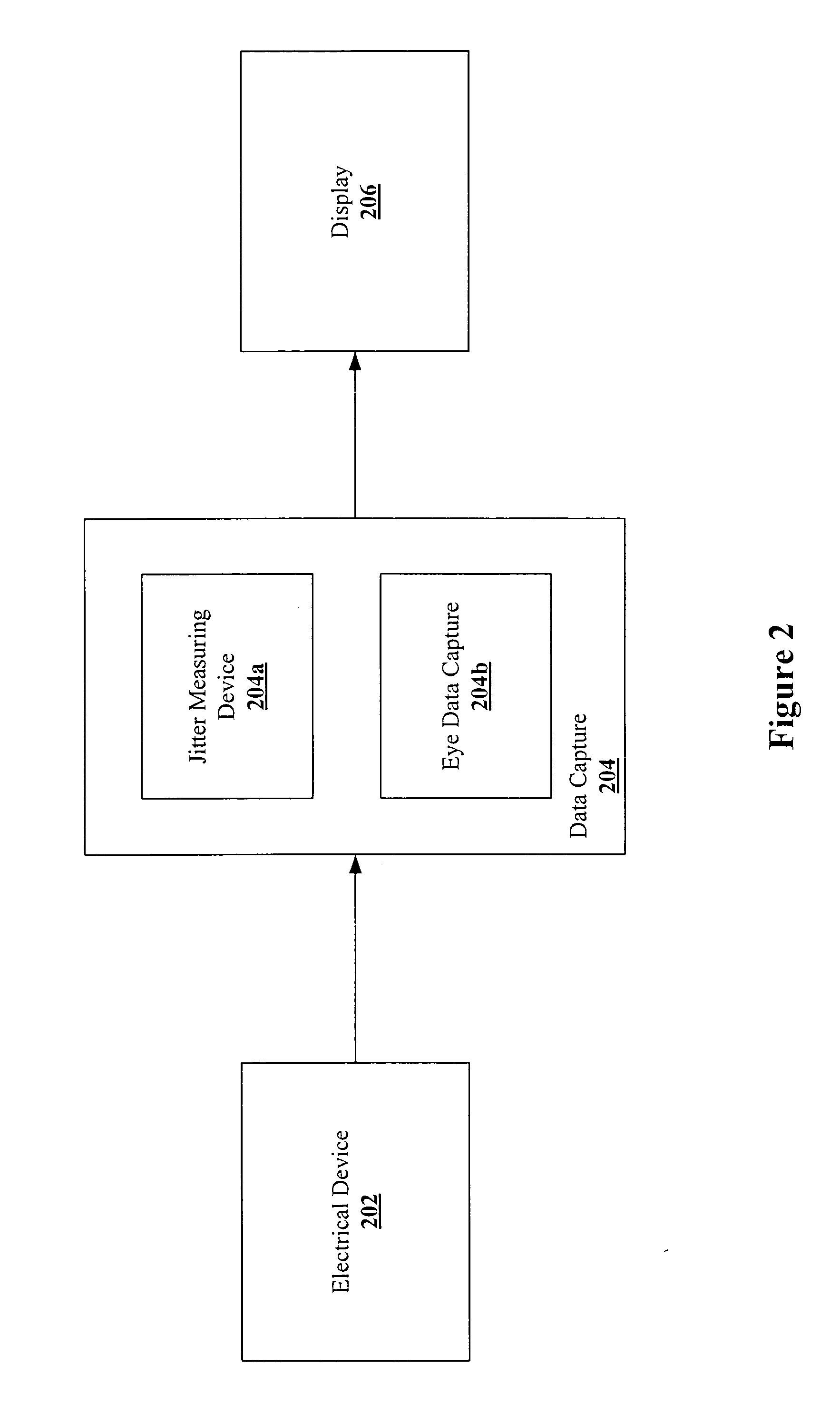
[0023] A system, apparatus and method for testing and optimizing an electrical device using a simultaneous display of both a signal's eye diagram and total jitter profile are described. In one embodiment of the invention, a data capture module capable of obtaining and separating the total jitter present in a signal into deterministic and random jitter, as well as other eye diagram information, is coupled to the electrical device and one or more display devices. These one or more display devices provide a user a simultaneous visual display of both random jitter and an eye diagram. This simultaneous display allows a user to test and optimize the electrical device without having to attach and detach the electrical device to multiple measuring devices. In one embodiment, the invention may be particularly applied to the characterization or simulation of a signal at a receiver.

[0024] In one embodiment of the invention, both the data capture module and the display(s) are integrated within...


PUM


Abstract

A system, apparatus and method for testing and optimizing an electrical device using a simultaneous display of both a signal's eye diagram and total jitter profile are described. In one embodiment of the invention, a data capture module capable of obtaining and separating the total jitter present in a signal into deterministic and random jitter, as well as other eye diagram information, is coupled to the electrical device and one or more display devices. These one or more display devices provide a user a simultaneous visual display of both random jitter and an eye diagram. This simultaneous display allows a user to test and optimize the electrical device without having to attach and detach the electrical device to multiple measuring devices.

Description

BACKGROUND [0001] A. Technical Field [0002] This invention relates generally to electrical device testing and optimization, and more particularly, to the measurement of jitter and the display of an eye diagram during the characterization of an electrical device. [0003] B. Background of the Invention [0004] The importance of electrical device testing and optimization is well known in the art. A number of different technological advancements have improved the performance of communication devices and led to ever-increasing rates at which data may be sent between electrical devices. These advancements have also given rise to a new era of electronic product verification and testing. In particular, the importance of properly measuring signal characteristics, such as a signal-to-noise ratio, jitter, and other signal integrity characteristics, may become even more important as communications systems become increasingly complex. [0005] Electrical components need to be tested and verified in ...

Claims


Application Information

Patent Timeline
Patent Type & Authority Applications(United States)
IPC IPC(8): G06F19/00
CPCG01R31/31709G01R13/0236
Inventor ROMERO, GABRIEL LEANDRO
Owner AVAGO TECH WIRELESS IP SINGAPORE PTE
Why Eureka
Try Eureka