Package for Image Sensor and Identification Module
a technology for identification modules and image sensors, applied in the field of packaging for image sensors and identification modules, can solve the problems of increasing cost and volume, and achieve the effects of improving image sensing quality, reducing process steps, and increasing function
- Summary
- Abstract
- Description
- Claims
- Application Information
AI Technical Summary
Benefits of technology
Problems solved by technology
Method used
Image
Examples
Embodiment Construction
[0016] To make it easier for understanding the objective of the invention, its innovative features and performance, a detailed description and technical characteristics of a package for an image sensor and an identification module are described together with the drawings as follows.
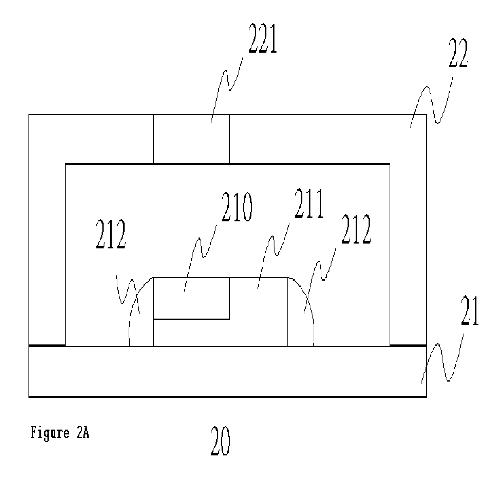
[0017] Referring to FIG. 2A and FIG. 2B, a schematic diagram and a top plan view illustrate a package for an image sensor and an identification module. The package for the image sensor and the identification module 20 comprises a substrate 21 and a holder 22. A System-on-Chip 211 having an image sensing device 210 is set on the substrate 21. The System-on-Chip 211 is mounted by a welding wire 212 on the substrate 21. The holder 22 is mounted by glue on the substrate 21 to seal the System-on-Chip 211. The holder 210 has a window 221 which is upon the image sensing device 210 to help the image sensing device 210 to receive an image. The holder 210 is an opaque material. The window 221 is glass or a transpa...
PUM
 Abstract
Description
Claims
Application Information


