Programmable Resistive RAM and Manufacturing Method

a technology of programmable resistive ram and manufacturing method, which is applied in the direction of semiconductor devices, semiconductor/solid-state device details, electrical apparatus, etc., can solve the problems of small programmable resistive ram cell and power consumption reduction, and achieve the effect of reducing cost, reducing the number or precision of photolithographic masks, and raising product yield

Active Publication Date: 2007-07-12
MACRONIX INT CO LTD
View PDF99 Cites 214 Cited by
  • Summary
  • Abstract
  • Description
  • Claims
  • Application Information

AI Technical Summary

Benefits of technology

[0029]In some embodiments, the method, or one or more of the steps, is a self-aligned process, such as the step of removing the upper portions of the interlayer contacts, and / or the step of forming the programmable resistive elements. The self-aligned feature reduces cost by reducing the number or precision of photolithographic masks, and correspondingly raises product yield.

Problems solved by technology

Accordingly, a smaller programmable resistive RAM cell is associated with decreased power consumption.
However, such a mask is associated with accompanying problems, such as proper alignment of the mask with the already fabricated layers of the planar integrated circuit.

Method used


Image

  • Programmable Resistive RAM and Manufacturing Method
  • Programmable Resistive RAM and Manufacturing Method
  • Programmable Resistive RAM and Manufacturing Method

Examples


Embodiment Construction

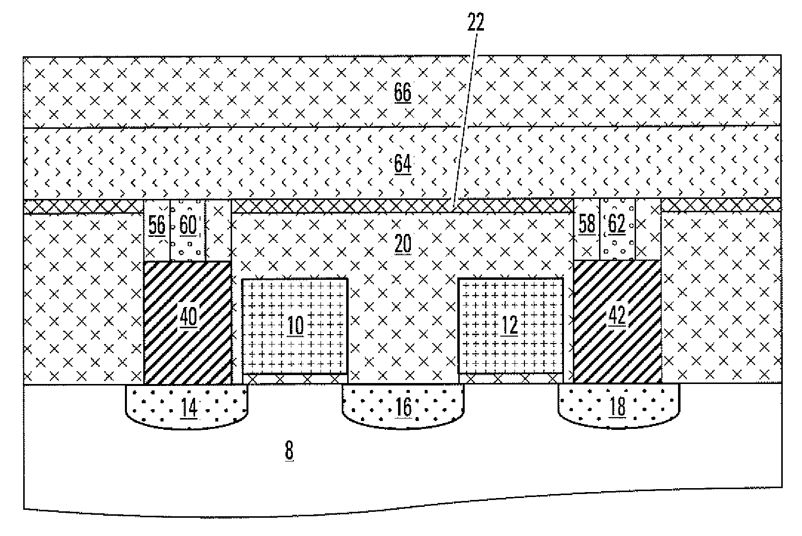
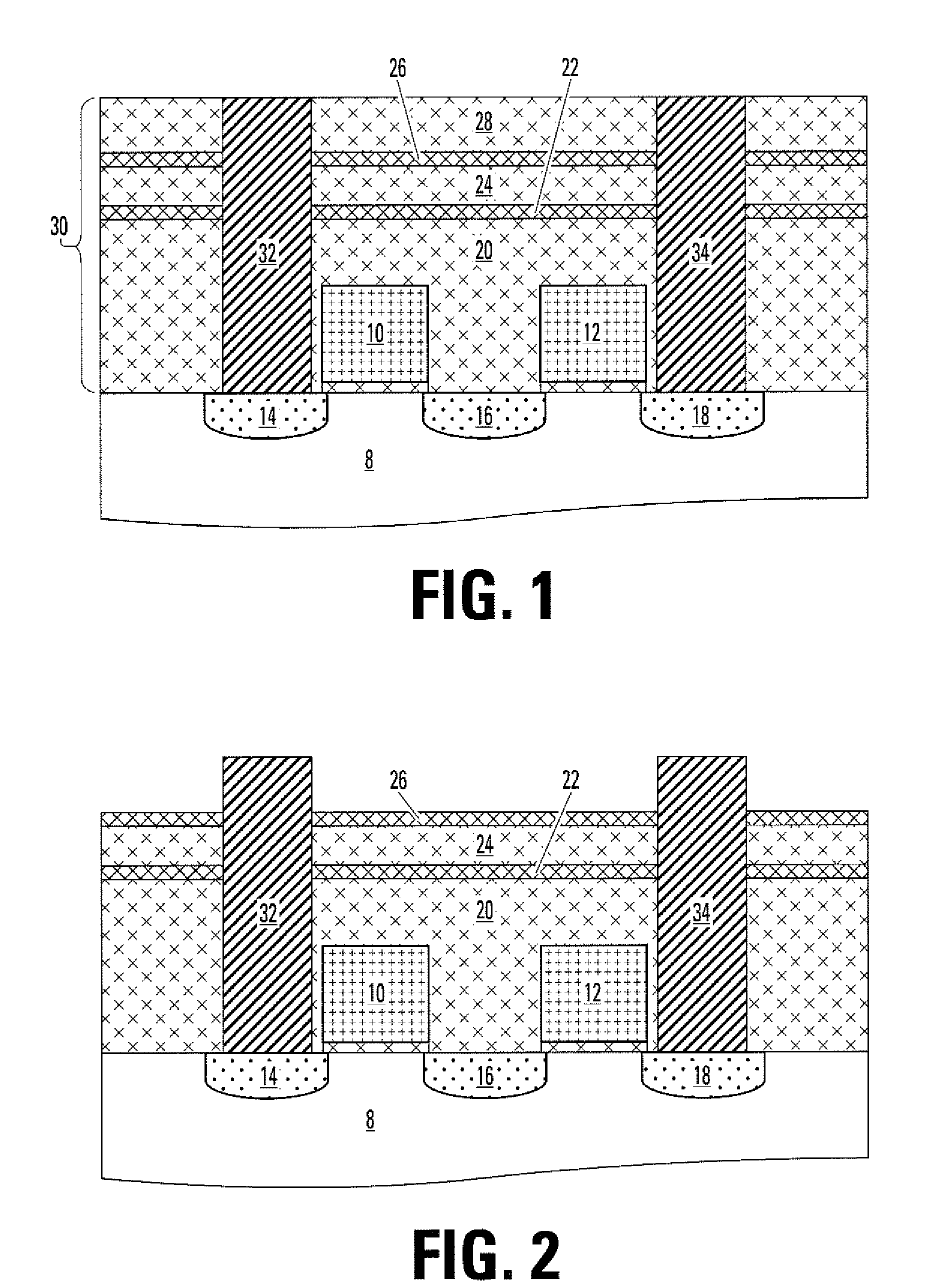
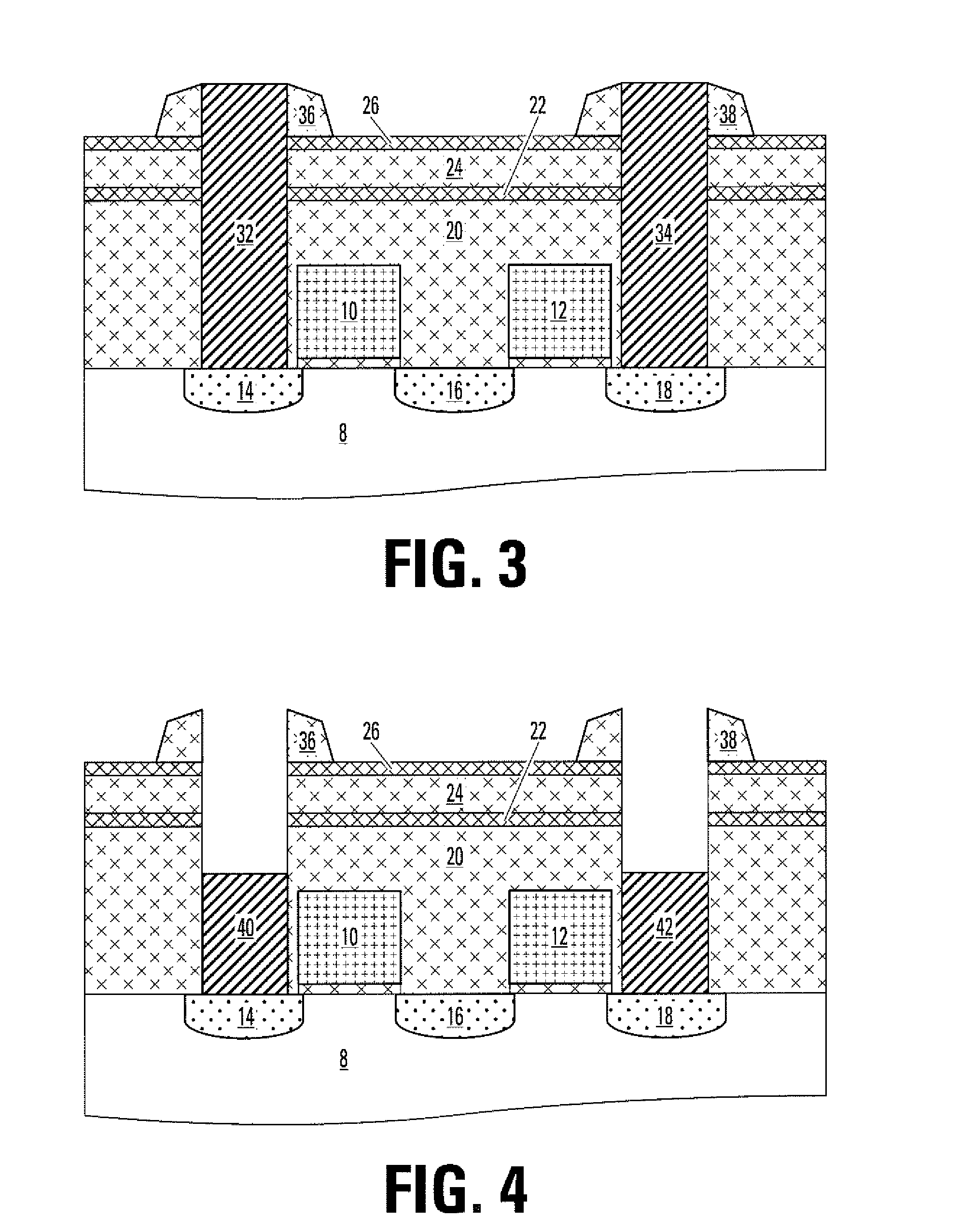
[0040]Various embodiments are directed at a manufacturing method for memory, such as nonvolatile embedded memory implementing programmable resistance RAM. Examples of resistance device RAM are resistance memory (RRAM), polymer memory, and phase change memory (PCRAM). The programmable resistive elements are formed to have a cross-section small than the cross-section of the upper portion of the interlayer contacts of programmable resistance RAM.

[0041]FIG. 1 is a cross-sectional view during the manufacturing process that shows the formation of the transistor circuitry, multiple dielectric layers, and interlayer contacts.

[0042]The substrate 8 (which may also be an n-well or p-well) has source and drain regions 14, 16, and 18. The gates 10 and 12 are conductive rows which selectively access the programmable resistive RAM cells, and induce a channel under the respective regions of the substrate 8 under the gates 10 and 12, between regions 14 and 16 and regions 16 and 18. Dielectric layers...


PUM


Abstract

Programmable resistive RAM cells have a resistance that depends on the size of the programmable resistive elements. Manufacturing methods and integrated circuits for programmable resistive elements with uniform resistance are disclosed that have a cross-section of reduced size compared to the cross-section of the interlayer contacts.

Description

REFERENCE TO RELATED APPLICATION[0001]This application claims the benefit of U.S. Provisional Patent Application No. 60 / 757,366, filed 9 Jan. 2006 by inventors ChiaHua Ho, Erh-Kun Lai and Kuang Yeu Hsieh entitled Process of Self-Align Formation of Bistable Resistance Random Access Memory.BACKGROUND OF THE INVENTION[0002]1. Field of the Invention[0003]The invention relates to integrated circuit nonvolatile memory. In particular, the invention relates to programmable resistive nonvolatile memory, such as phase change memory.[0004]2. Description of Related Art[0005]Nonvolatile memory stores data without requiring a continuous supply of power. Programmable resistive memory such as phase change memory is an example of nonvolatile memory. A high current reset electrical pulse melts and quenches the programmable resistive element into an amorphous state, raising the resistance of the programmable resistive element. A low current set electrical pulse crystallizes and lowers the resistance o...

Claims


Application Information

Patent Timeline
Patent Type & Authority Applications(United States)
IPC IPC(8): H01L27/10H01L21/82
CPCH01L27/24H01L27/101H10B63/00
Inventor HO, CHIAHUALAI, ERH KUNHSIEH, KUANG YEU
Owner MACRONIX INT CO LTD
Why Eureka
Try Eureka