Circuit Board with Conductive Structure and Method for Fabricating the same

a technology of conductive structure and circuit board, which is applied in the direction of printed circuit manufacturing, printed circuit aspects, basic electric elements, etc., can solve the problems of circuit line already being etched away, the speed of chemical etching cannot be easily controlled, and the quality and stability of electrical connection of the circuit board is already degraded, so as to enhance the electrical quality and stability of the circuit board, the effect of high ductility and high combining strength

Inactive Publication Date: 2007-07-12
PHOENIX PRECISION TECH CORP
View PDF7 Cites 14 Cited by
  • Summary
  • Abstract
  • Description
  • Claims
  • Application Information

AI Technical Summary

Benefits of technology

[0009]In the light of forgoing drawbacks, an objective of the present invention is to provide a circuit board with a conductive structure and its fabricating method that avoids layering or fractures at the bottom of the conductive structure so as to enhance the quality and reliability of electrically connection of the circuit board.
[0010]Another objective of the present invention is to provide a circuit board with a conductive structure and its fabricating method that reinforces the combing strength between an electrically connecting pad on a circuit layer with the conductive structure on another circuit layer.
[0011]Still another objective of the present invention is to provide a circuit board with a conductive structure and its fabricating method that enhances the electroplating quality and reliability of the conductive structure.
[0018]Compared to the prior art, the present invention forms a buffer metal layer on the electrically connecting pad of the first circuit layer. Since the material of the buffer metal layer is characterized by high combining strength and high ductility, it can be easily combined with the electrically connecting pad or the subsequently formed conductive structure. Thus, the combining strength of the conductive structure and the electrically connecting pad is reinforced by the buffer metal layer. In addition, layering or fractures at the bottom of the conductive structure causing open circuit or micro open circuit can be avoided, therefore enhancing the electrical quality and stability of the circuit board.
[0019]Moreover, since the buffer metal layer covers and protects the electrically connecting pad underneath, the electrically connecting pad is avoided from over etching during a micro-etching process, thus enhancing the electroplating quality and reliability of the subsequently formed conductive structure.

Problems solved by technology

This may cause open circuit or micro open circuit and severely degrades the quality and stability of electrically connection of the circuit board.
During micro-etching, since the width of the circuit line is usually smaller that that of the electrically connecting pad and the speed of chemical etching cannot be easily controlled, the circuit line may already be etched away when the electrically connecting pad reaches a proper roughness.
Conversely, if the chemical etching time is reduced to avoid overly etching the circuit line, the surface of the electrically connecting pad may not be rough enough, reducing the combining strength between the conductive blind via and the electrically connecting pad.
Accordingly, aforementioned problems of open circuit or micro open circuit may easily occur.

Method used


Image

  • Circuit Board with Conductive Structure and Method for Fabricating the same
  • Circuit Board with Conductive Structure and Method for Fabricating the same
  • Circuit Board with Conductive Structure and Method for Fabricating the same

Examples


first embodiment

[0027]An embodiment of the method for fabricating circuit board with conductive structure of the present invention is illustrated in detail below in conjunction with FIGS. 2A to 2D.

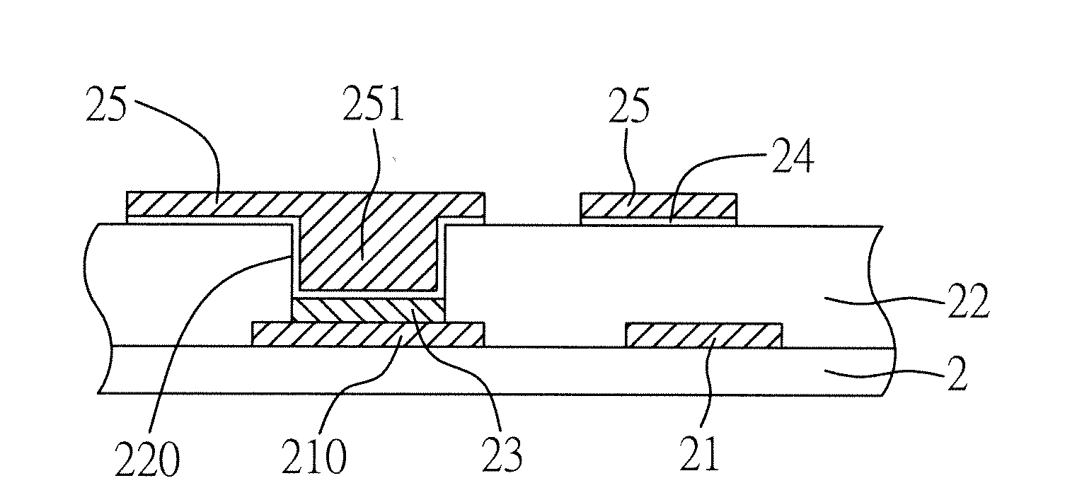
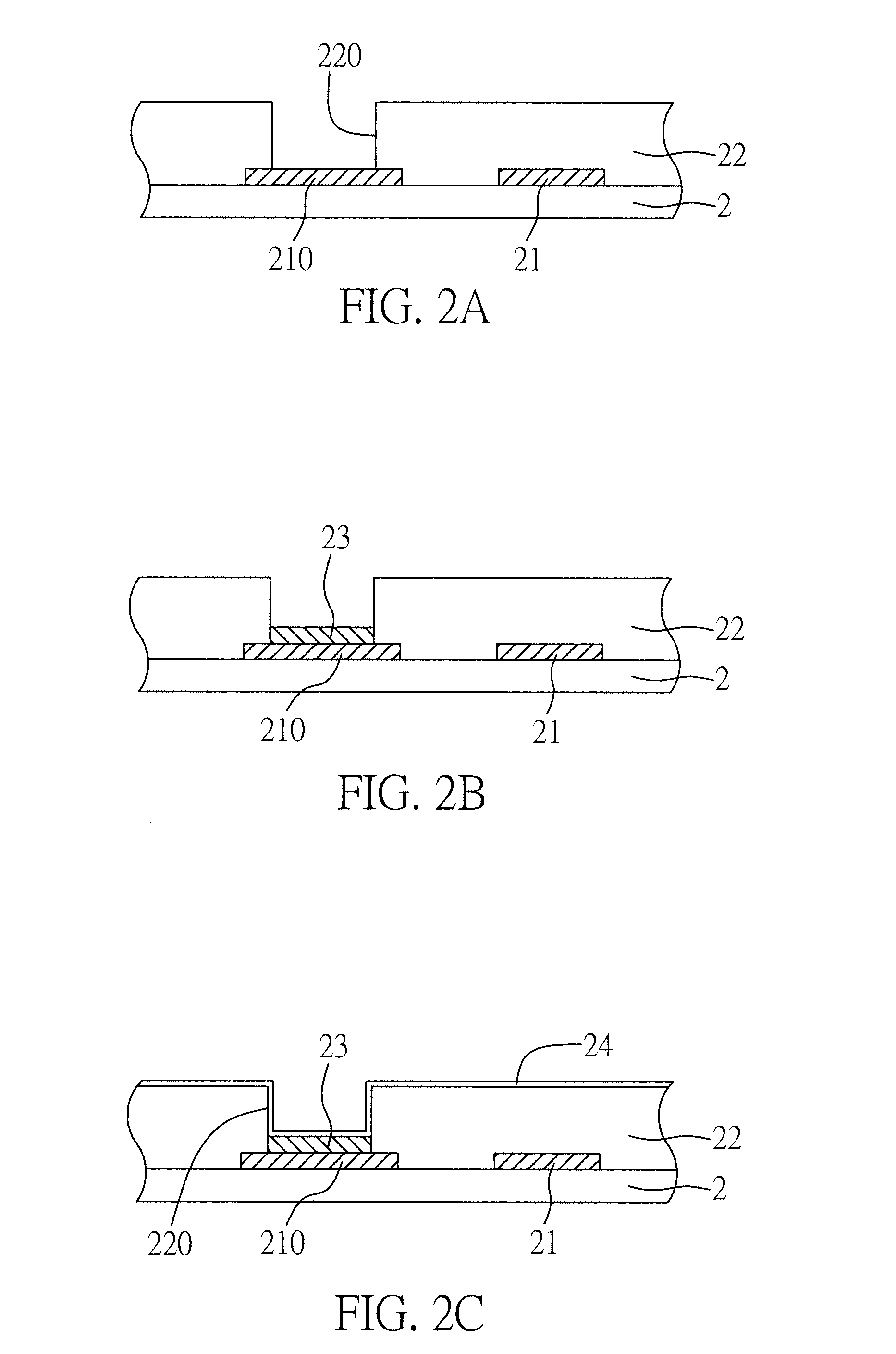
[0028]Referring to FIG. 2A, first, a circuit board 2 is provided which has at least a circuit layer 21 with at least an electrically connecting pad 210. A dielectric layer 22 is formed on the surface of the circuit board 2 and the circuit layer, wherein a via 220 is formed at a location corresponding to the electrically connecting pad 210 of the circuit layer 21 for exposing the electrically connecting pad 210. The electrically connecting pad may electrically conduct an inner circuit (not shown) of the circuit board 2 via a conductive structure (not shown).

[0029]Referring next to FIG. 2B, a buffer metal layer 23 is formed on the electrically connecting pad 210 within the via 220 of the dielectric layer 22. In this embodiment, the buffer metal layer 23 is formed using electroless plating, such as chemical ...

second embodiment

[0033]Another embodiment of the method for fabricating circuit board with conductive structure of the present invention is illustrated in conjunction with FIGS. 3A to 3C. This embodiment is different from the first embodiment in that the conductive layer is first formed in the via of the dielectric layer and the buffer metal layer and the conductive structure are formed on the surface of the conductive layer thereafter.

[0034]Referring to FIG. 3A, first, at least a circuit layer 21 is formed on the circuit board 2. The circuit layer 21 has at least an electrically connecting pad 210. A dielectric layer 22 is formed on the surface of the circuit board 2 and the circuit layer, wherein a via 220 is formed at a location corresponding to the electrically connecting pad 210 of the circuit layer 21 for exposing the electrically connecting pad 210. Then, a conductive layer 24 is formed on the surface of the dielectric layer 22 and its via 220 so that the conductive layer 24 is electrically c...


PUM

PropertyMeasurementUnit
thicknessaaaaaaaaaa
conductiveaaaaaaaaaa
dielectricaaaaaaaaaa

Abstract

A method for fabricating a circuit board with a conductive structure and the same are proposed. A buffer metal layer is formed on an electrically connecting pad of a circuit layer of a circuit board in advance. A conductive structure is then formed on the buffer metal layer to form the conductive structure of the present invention and is connected to the circuits located in the different layers of the circuit board. The combining strength of the conductive structure and the electrically connecting pad is reinforced by the buffer metal layer as the buffer metal layer has high ductility. The long-term electrical quality and stability are also enhanced.

Description

FIELD OF THE INVENTION[0001]The present invention relates to circuit boards with conductive structures and a method for fabricating the same, and more particularly, to a circuit board with a conductive blind via and a method for fabricating the same.BACKGROUND OF THE INVENTION[0002]Circuit designs for circuit boards and packaging substrates tend to become denser in order to meet the demands for miniaturization and increased functionalities of electronic products. Accordingly, multi-layer circuit board with thin circuits and high density is the trend for the next generation. Conductive structures for electrically connecting circuit layers in a multi-layer circuit board are one of the main factors that affect the quality for electrically connection of the circuit board.[0003]Traditionally, conductive blind vias are employed for connection between the circuit layers of a circuit board, as shown in FIGS. 1A to 1C. First referring to FIG. 1A, a dielectric layer 12 is formed on a circuit ...

Claims


Application Information

Patent Timeline
Patent Type & Authority Applications(United States)
IPC IPC(8): H01L23/48H01L21/44
CPCH01L21/486H01L23/49827H05K3/421H05K2201/0338H05K2201/0341H01L2924/0002H05K2201/09563H01L2924/00
Inventor HSU, SHIH-PING
Owner PHOENIX PRECISION TECH CORP
Why Eureka
Try Eureka