Method for manufacturing 3D NAND memory using gate replacement, and resulting structures

a gate replacement and nand memory technology, applied in the field of memory, can solve the problems of increasing resistance, requiring higher power word line drivers, and slow operating speeds, and achieve the effect of improving the operating characteristics of 3d memory

Active Publication Date: 2018-08-07
MACRONIX INT CO LTD
View PDF61 Cites 13 Cited by
  • Summary
  • Abstract
  • Description
  • Claims
  • Application Information

AI Technical Summary

Benefits of technology

[0008]A memory device and a method for manufacturing a memory device are described which can improve the operating characteristics of 3D memory. In one embodiment, the memory device includes a plurality of memory cells, and comprises a plurality of vertical pillars composed of a vertical channel and a multila

Problems solved by technology

One problem associated with 3D memory structures arises because the word lines of stacked thin strips of polysilicon have relatively high resistance, and the resistance increases as the sizes of the structures shrink.
Higher resistance word lines can result in slower operating speeds, and require higher power word line drivers.
Although one approach to r

Method used


Image

  • Method for manufacturing 3D NAND memory using gate replacement, and resulting structures
  • Method for manufacturing 3D NAND memory using gate replacement, and resulting structures
  • Method for manufacturing 3D NAND memory using gate replacement, and resulting structures

Examples


Embodiment Construction

[0035]A detailed description of embodiments of the present invention is provided with reference to the FIGS. 1-21.

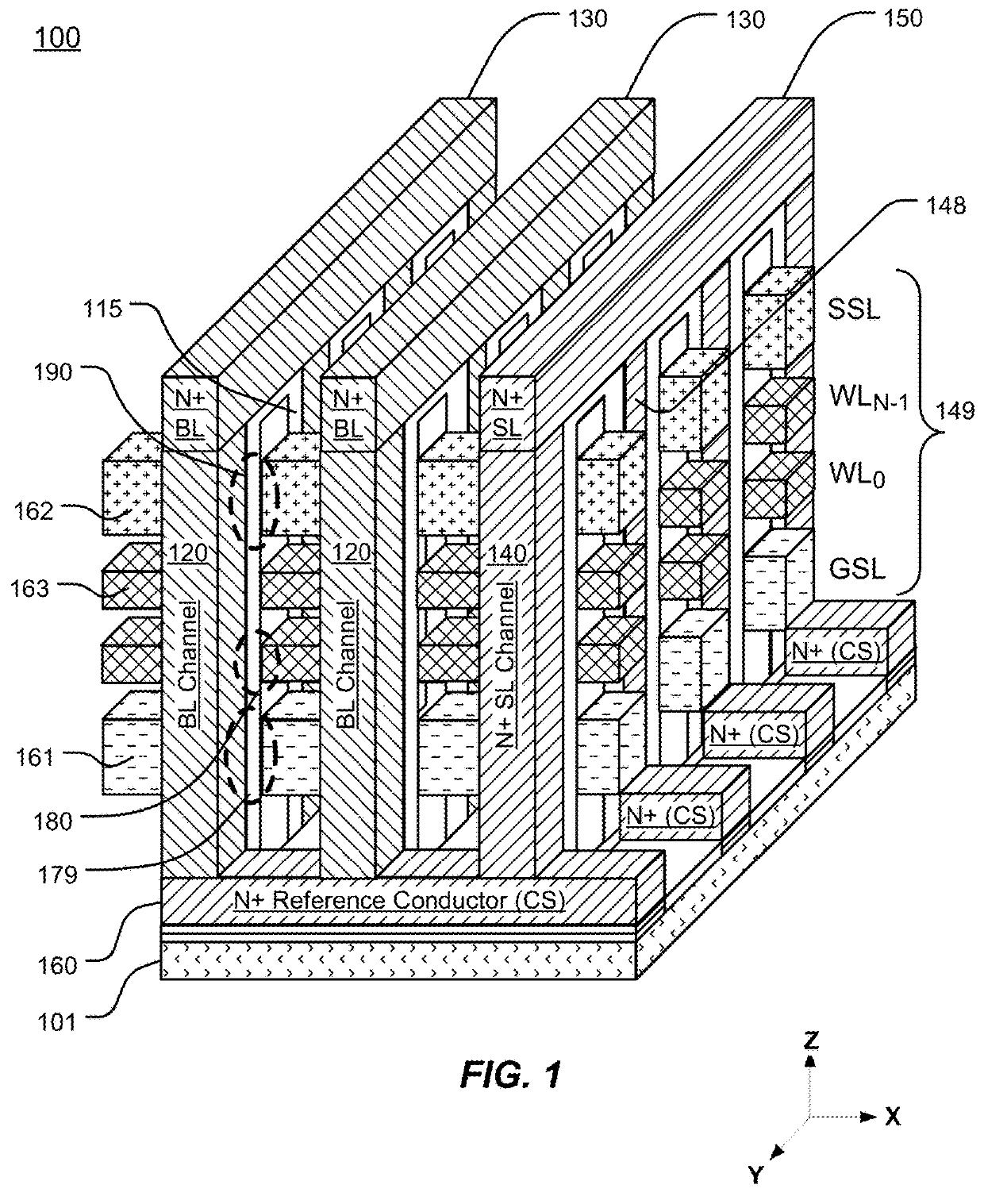
[0036]FIG. 1 is a perspective diagram of a three-dimensional 3D memory device 100 having an independent double gate structure with dielectric lined word lines, based on 3D vertical channel technology having a structure as described in U.S. Pat. No. 9,147,468, entitled MULTIPLE-BIT-PER-CELL, INDEPENDENT DOUBLE GATE, VERTICAL CHANNEL MEMORY, by H. T. Lue, issued 29 Sep. 2015, which is incorporated by reference as if fully set forth herein.

[0037]The memory device 100 includes an array of NAND strings of memory cells, configured in an independent double gate vertical channel memory array (IDGVC) with two NAND strings per vertical channel, and suitable for multiple-bit-per-cell data storage. The memory device 100 includes an integrated circuit substrate, and a plurality of stacks of conductive strips separated by insulating material, including at least a bottom plane of condu...


PUM


Abstract

A 3D memory device includes a plurality of vertical pillars composed of a vertical channel and a multilayer data storage structure. The multilayer data storage structure can comprise a dielectric charge trapping structure. A stack of dielectric lined conductive strips separated in the stack by insulating strips have sidewalls disposed adjacent the corresponding vertical pillars. The conductive strips have a dielectric liner having a dielectric constant κ greater than 7 on the sidewalls in contact with the outside layer of the multilayer data storage structure on the corresponding pillar. The conductive strips in embodiments described herein can comprise a relatively low resistance material, such as a metal or a metal nitride. A manufacturing method using Si—Ge selective etching of sacrificial layers can be used in a gate replacement process to form the dielectric conductive strips.

Description

BACKGROUNDField of the Invention[0001]The present invention relates to memories, and particularly relates to 3D NAND memories.Description of Related Art[0002]As critical dimensions of devices in integrated circuits shrink to the limits of common memory cell technologies, designers have been looking to techniques for stacking multiple planes of memory cells to achieve greater storage capacity, and to achieve lower costs per bit. For example, thin-film transistor techniques are applied to charge trapping memory technologies in Lai, et al., “A Multi-Layer Stackable Thin-Film Transistor (TFT) NAND-Type Flash Memory,” IEEE Int'l Electron Devices Meeting, 11-13 Dec. 2006; and in Jung et al., “Three Dimensionally Stacked NAND Flash Memory Technology Using Stacking Single Crystal Si Layers on ILD and TANOS Structure for Beyond 30 nm Node,” IEEE Int'l Electron Devices Meeting, 11-13 Dec. 2006.[0003]Another structure that provides vertical NAND cells in a charge trapping memory technology is ...

Claims


Application Information

Patent Timeline
IPC IPC(8): H01L27/11H01L27/11582H01L27/11565H01L23/528H01L27/11575H01L21/82H01L23/52H01L27/11578H01L27/11573H01L27/11551H01L27/11524H01L21/8239H01L29/792H01L29/66H01L29/788G11C16/04
CPCH01L27/11582H01L27/11565H01L23/5283H01L27/11573H01L27/11578H01L27/11575H01L29/66833H01L27/11524H01L21/8239G11C2211/4016G11C16/0483H01L27/11551G11C2213/75G11C2213/71H01L29/7926H01L29/7889H10B41/35H10B43/35H10B43/27H10B43/20H10B43/40H10B43/50H10B41/20H10B99/00
Inventor LAI, ERH-KUNLUNG, HSIANG-LAN
Owner MACRONIX INT CO LTD
Why Eureka
Try Eureka