Method of cleaning wafer and method of manufacturing gate structure

a technology of cleaning wafers and gate structures, which is applied in the direction of semiconductor devices, electrical equipment, basic electric elements, etc., can solve the problems of direct influence of gate structures on the subsequent yield, reliability and performance of devices, and the quality and reliability of subsequently formed devices, so as to improve the overall yield of wafers

Active Publication Date: 2006-08-03
UNITED MICROELECTRONICS CORP
View PDF10 Cites 13 Cited by
  • Summary
  • Abstract
  • Description
  • Claims
  • Application Information

AI Technical Summary

Benefits of technology

[0008] Accordingly, one objective of the present invention is to provide a method of cleaning a wafer. The method is capable of removing residues on the surface of the wafer and improving overall yield of the wafer.
[0009] Another objective of the present invention is to provide a method of fabricating gate structures on a wafer in which residues on the wafer can be efficiently removed to improve the quality and reliability of devices.
[0013] In the present invention, phosphoric acid solution and hydrofluoric acid solution are used to clean the substrate. Since phosphoric acid solution is effective in removing the silicon nitride residues formed in a reaction between the nitrogen-containing barrier layer and the silicon-containing gate layer, the gate dielectric layer residues retained due to the overlying silicon nitride residues can be avoided. Consequently, the yield of the wafer as well as the quality and reliability of the devices within the wafer can be improved.

Problems solved by technology

The quality of the gate structures directly affects the subsequent yield, reliability and performance of a device.
As a result, these residues on the wafer will affect the quality and reliability of the subsequently formed devices.

Method used


Image

  • Method of cleaning wafer and method of manufacturing gate structure
  • Method of cleaning wafer and method of manufacturing gate structure
  • Method of cleaning wafer and method of manufacturing gate structure

Examples


Embodiment Construction

[0020] Reference will now be made in detail to the present embodiments of the invention, examples of which are illustrated in the accompanying drawings. Wherever possible, the same reference numbers are used in the drawings and the description to refer to the same or like parts.

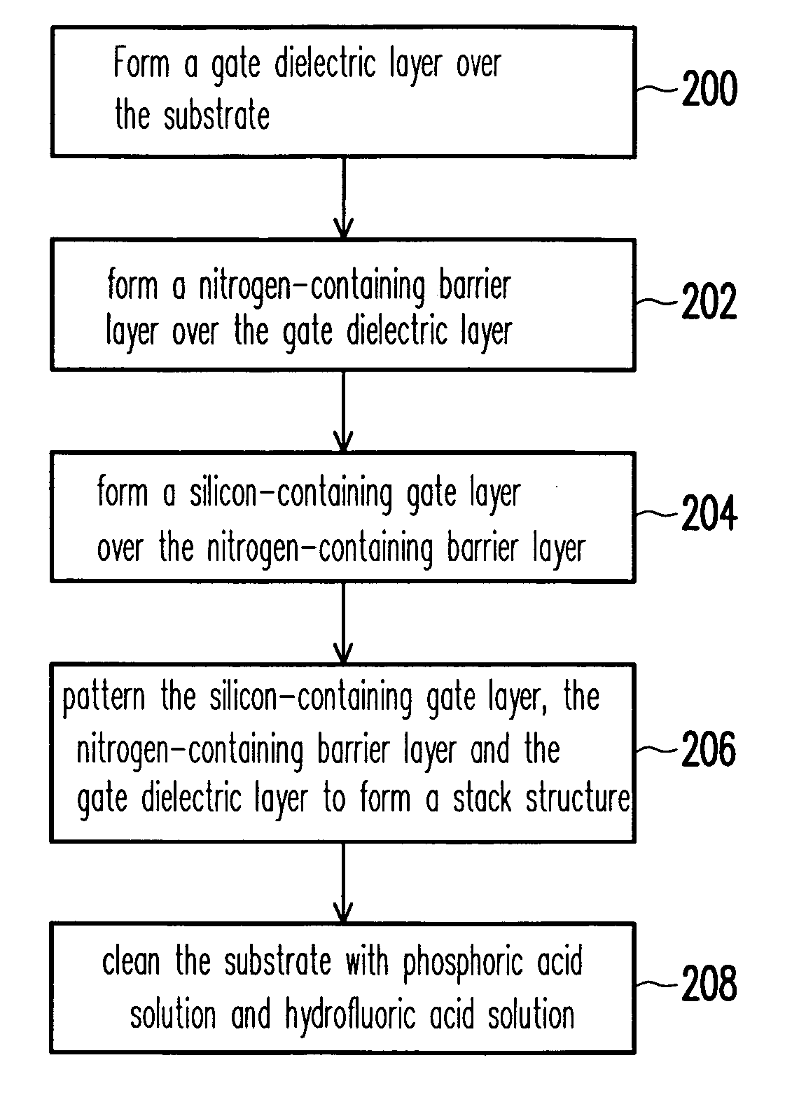
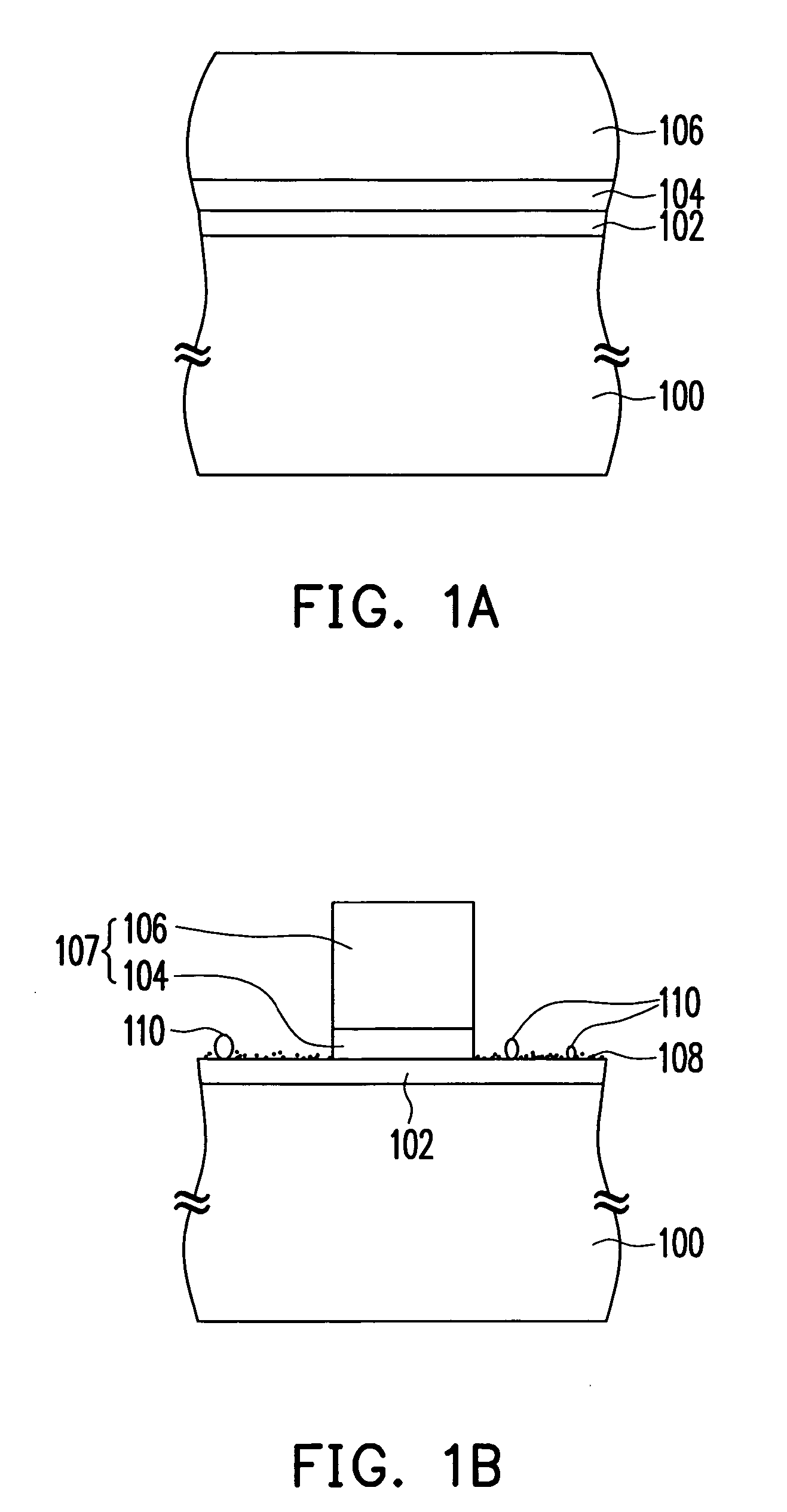
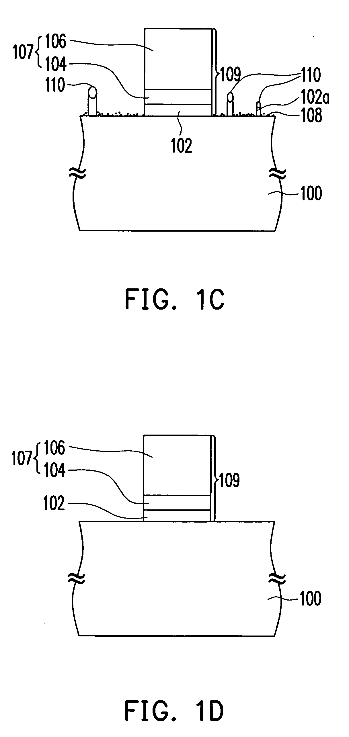
[0021]FIGS. 1A through 1D are schematic cross-sectional views showing the steps for fabricating a gate structure according to one embodiment of the present invention. FIG. 2 is a flowchart showing the steps carried out in FIGS. 1A through 1D. As shown in FIGS. 1A and 2, a gate dielectric layer 102 is formed over a substrate 100 (in step 200). The gate dielectric layer 102 is fabricated using a high dielectric constant material such as hafnium dioxide, nitrogen doped hafnium dioxide, nitrogen and silicon doped hafnium dioxide, silicon doped hafnium dioxide and so on. The gate dielectric layer 102 is formed, for example, by performing an atomic layer deposition (ALD) process, a metal-organic chemical vapor dep...


PUM

PropertyMeasurementUnit
temperatureaaaaaaaaaa
dielectric constantaaaaaaaaaa
scanning electron microscopeaaaaaaaaaa

Abstract

A method of cleaning a wafer, adapted for a patterned gate structure. The gate structures comprise a gate dielectric layer, a nitrogen-containing barrier layer and a silicon-containing gate layer sequentially stacked over the substrate. The method includes cleaning the substrate with phosphoric acid solution and hydrofluoric acid solution so that silicon nitride residues formed in a reaction between the nitrogen-containing barrier layer and the silicon-containing gate layer can be removed and the amount of pollutants and particles can be reduced. Ultimately, the yield of the process as well as the quality and reliability of the device are improved.

Description

BACKGROUND OF THE INVENTION [0001] 1. Field of the Invention [0002] The present invention relates to a semiconductor fabrication process. More particularly, the present invention relates to a method of cleaning wafers and a method of manufacturing gate structures on wafers. [0003] 2. Description of the Related Art [0004] In the current semiconductor fabricating process, cleaning the wafer is one of the most important and frequent steps. The purpose of cleaning the wafer is to remove residues such as particles, organics or inorganic metallic ions from the surface. Hence, wafer cleaning is one of the critical factors affecting the yield as well as the quality and reliability of a device. [0005] On the other hand, the fabrication of gate structures on a wafer is also an important process in the semiconductor fabricating process. The quality of the gate structures directly affects the subsequent yield, reliability and performance of a device. Therefore, how to achieve a high degree of c...

Claims


Application Information

Patent Timeline
Patent Type & Authority Applications(United States)
IPC IPC(8): H01L21/336H01L21/302H01L21/461
CPCH01L21/0206H01L21/02071H01L21/28088H01L21/28194H01L29/4966H01L29/517H01L29/518
Inventor WU, CHIH-NINGLEE, CHARLIE CJLIAO, KUAN-YANG
Owner UNITED MICROELECTRONICS CORP
Why Eureka
Try Eureka