Semiconductor device and method for manufacturing the same

a technology of semiconductors and semiconductors, applied in the direction of semiconductor devices, electrical devices, transistors, etc., can solve the problem of difficult to achieve the optimal amount of signal b>5/b>vth

Inactive Publication Date: 2007-07-19
KK TOSHIBA
View PDF13 Cites 142 Cited by
  • Summary
  • Abstract
  • Description
  • Claims
  • Application Information

AI Technical Summary

Problems solved by technology

However, for the bulk substrate, it is difficult to accomplish the optimal amount of signal 5Vth, since the amount of the capacitance Cpn is small.

Method used


Image

  • Semiconductor device and method for manufacturing the same
  • Semiconductor device and method for manufacturing the same
  • Semiconductor device and method for manufacturing the same

Examples


first embodiment

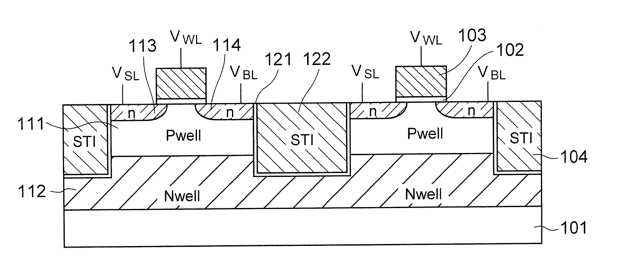
[0025]FIG. 1 is a side cross-sectional view of a semiconductor memory device according to a first embodiment. The semiconductor memory device shown in FIG. 1 includes capacitorless DRAM memory cells. A transistor constituting the DRAM memory cell shown in FIG. 1 is an FET (here, a MOSFET).

[0026]The semiconductor memory device shown in FIG. 1 includes a substrate 101, a gate oxide film 102 constituting the MOSFET, a gate electrode 103 constituting the MOSFET, a plurality of rows of STIs (Shallow Trench Isolations) 104 corresponding to a particular example of isolation layers for isolating MOSFET from one another. The gate oxide film 102 is a particular example of a gate insulator film of the transistor, and the gate electrode 103 is a particular example of a gate electrode of the transistor.

[0027]The substrate 101 is a bulk substrate (here, a bulk silicon substrate). The substrate 101 includes a p-type well (Pwell) 111 for storing signal charges corresponding to a particular example ...

second embodiment

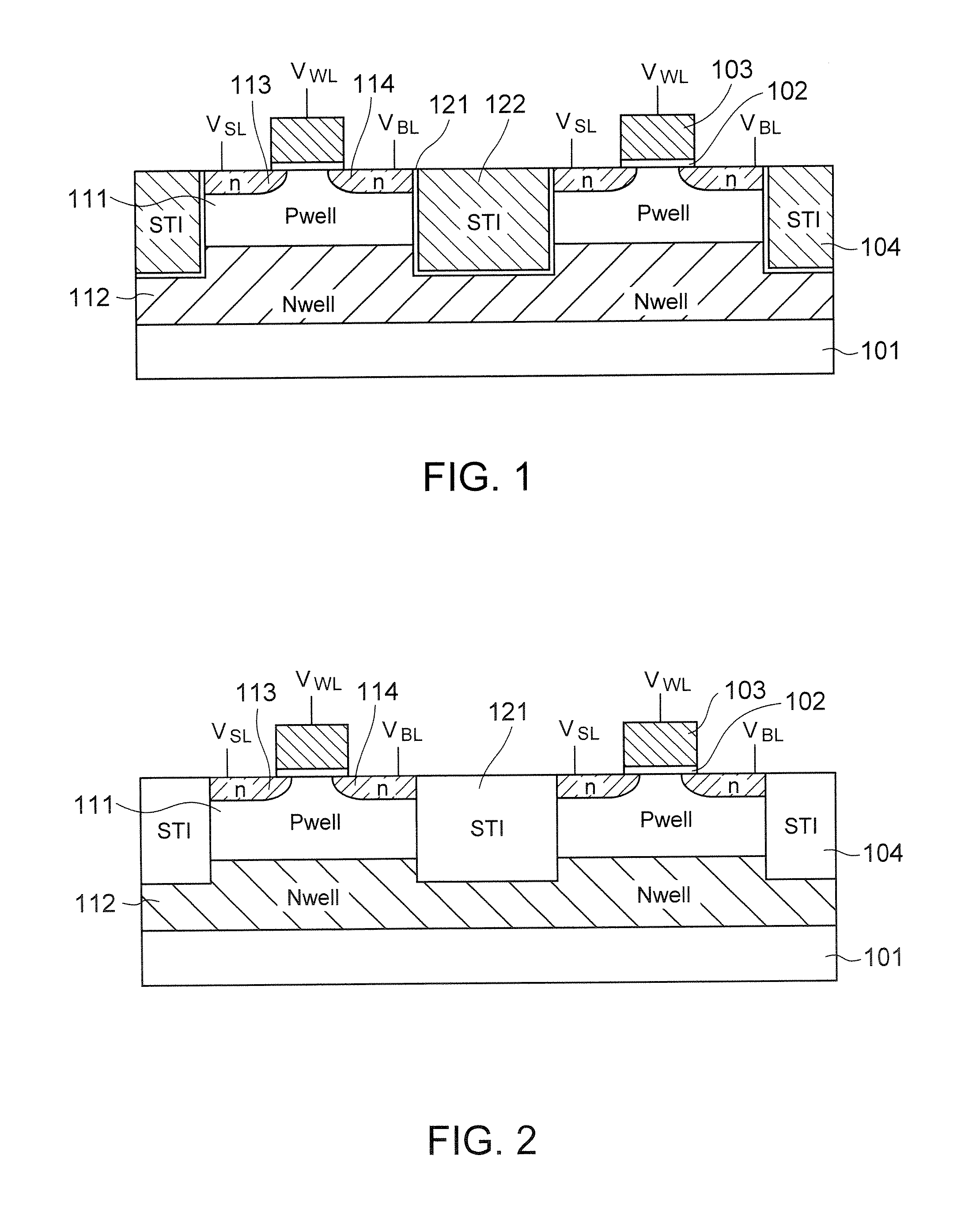
[0043]FIG. 8 is a side cross-sectional view of a semiconductor memory device of a second embodiment. Now, difference between the semiconductor memory device of the first embodiment in FIG. 1 and that of the second embodiment in FIG. 8 will be described.

[0044]In both the semiconductor memory devices in FIG. 1 and 8, each STI 104 has an insulating film 121 and a conductive layer 122. However, in the semiconductor memory device in FIG. 1, each STI 104 has the bottom surface and the side surfaces formed by the insulating film 121, and on the contrary, in the semiconductor memory device in FIG. 8, each STI 104 has the side surfaces formed by the insulating film 121 and the bottom surface formed by the conductive layer 122. Therefore, in the semiconductor memory device in FIG. 1, the conductive layer 122 of each STI 104 is electrically insulated from the substrate 101, while in the semiconductor memory device in FIG. 8, the conductive layer 122 of each STI 104 is electrically connected to...


PUM


Abstract

A semiconductor device of one embodiment of the present invention includes a substrate; isolation layers, each of which is formed in a trench formed on the substrate and has an insulating film and a conductive layer; a semiconductor layer of a first conductivity type for storing signal charges, formed between the isolation layers and isolated from the conductive layers by the insulating films; a semiconductor layer of a second conductivity type, formed under the semiconductor layer of the first conductivity type; and a transistor having a gate insulator film formed on the semiconductor layer of the first conductivity type and a gate electrode formed on the gate insulator film.

Description

CROSS REFERENCE TO RELATED APPLICATIONS[0001]This application is based upon and claims the benefit of priority from prior Japanese Patent Application No. 2006-8638, filed on Jan. 17, 2006, the entire contents of which are incorporated herein by reference.BACKGROUND OF THE INVENTION[0002]1. Field of the Invention[0003]This invention relates to a semiconductor device and method for manufacturing it, for example to a semiconductor memory device including capacitorless DRAM memory cells and a method for manufacturing it.[0004]2. Related Art[0005]A conventional DRAM memory cell of a DRAM includes a capacitor for storing signal charges and a switching transistor (for example, a MOSFET or other FETs) Capacitance of the capacitor required to store signal charges is generally about 30 fF. It is necessary to keep this capacitance of the capacitor of about 30 fF for a DRAM to maintain stable operation, even if the reduced design rule for the DRAM is adopted due to improvement in a degree of ce...

Claims


Application Information

Patent Timeline
Patent Type & Authority Applications(United States)
IPC IPC(8): H01L29/792
CPCH01L27/108H01L29/7841H01L27/10802H10B12/20H10B12/00
Inventor HAMAMOTO, TAKESHI
Owner KK TOSHIBA
Why Eureka
Try Eureka