Method and apparatus for buffering graphics data in a graphics system
a graphics system and graphics data technology, applied in the field of computer graphics, can solve the problems of complex computer graphics generation, unable to actually interact with the computer doing the graphics generation, and limited computer-generated three-dimensional graphics a few years ago, so as to reduce the synchronization requirements of consumers and efficiently buffer graphics commands. , the effect of increasing flexibility
- Summary
- Abstract
- Description
- Claims
- Application Information
AI Technical Summary
Benefits of technology
Problems solved by technology
Method used
Image
Examples
example graphics
Pipeline
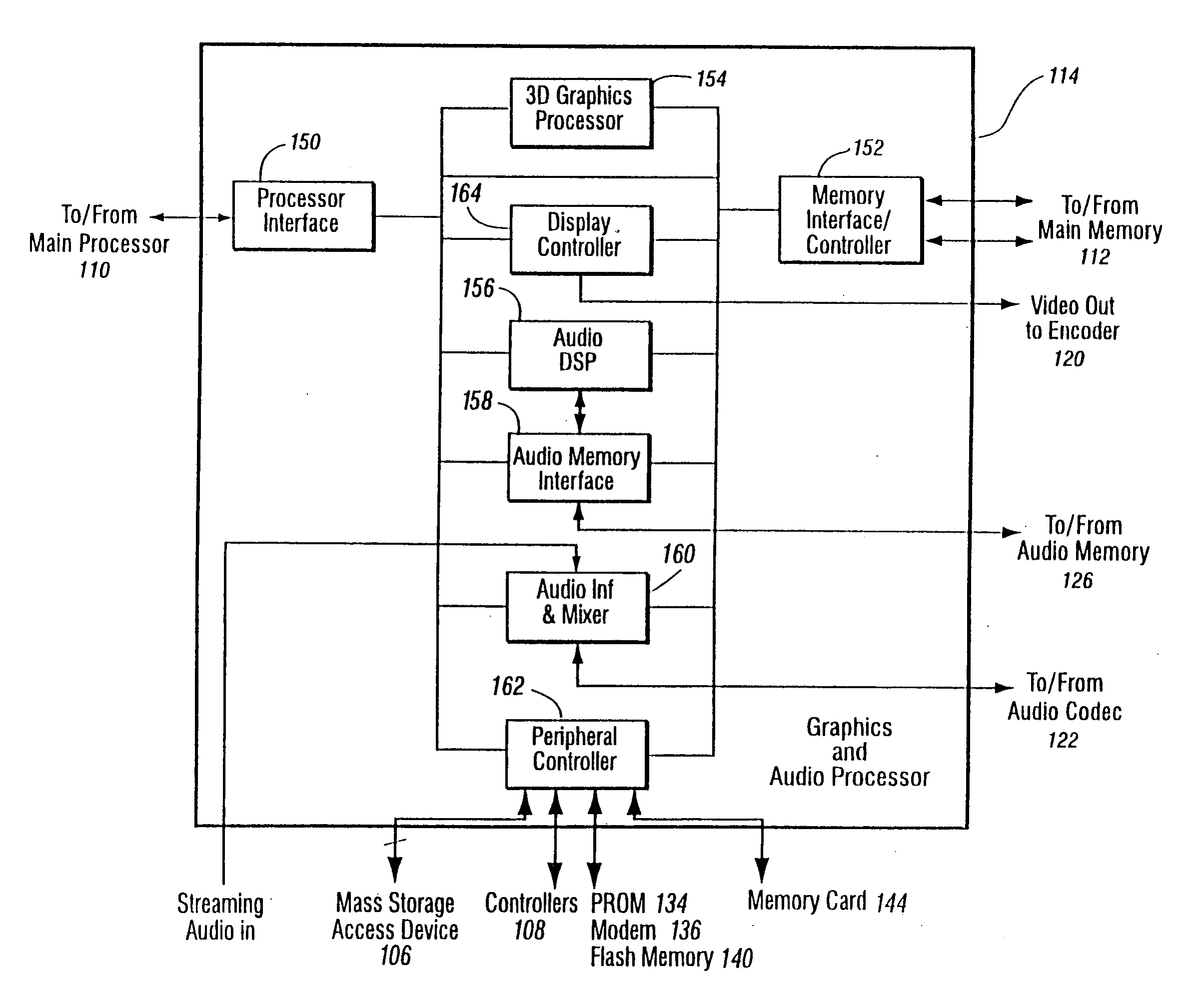
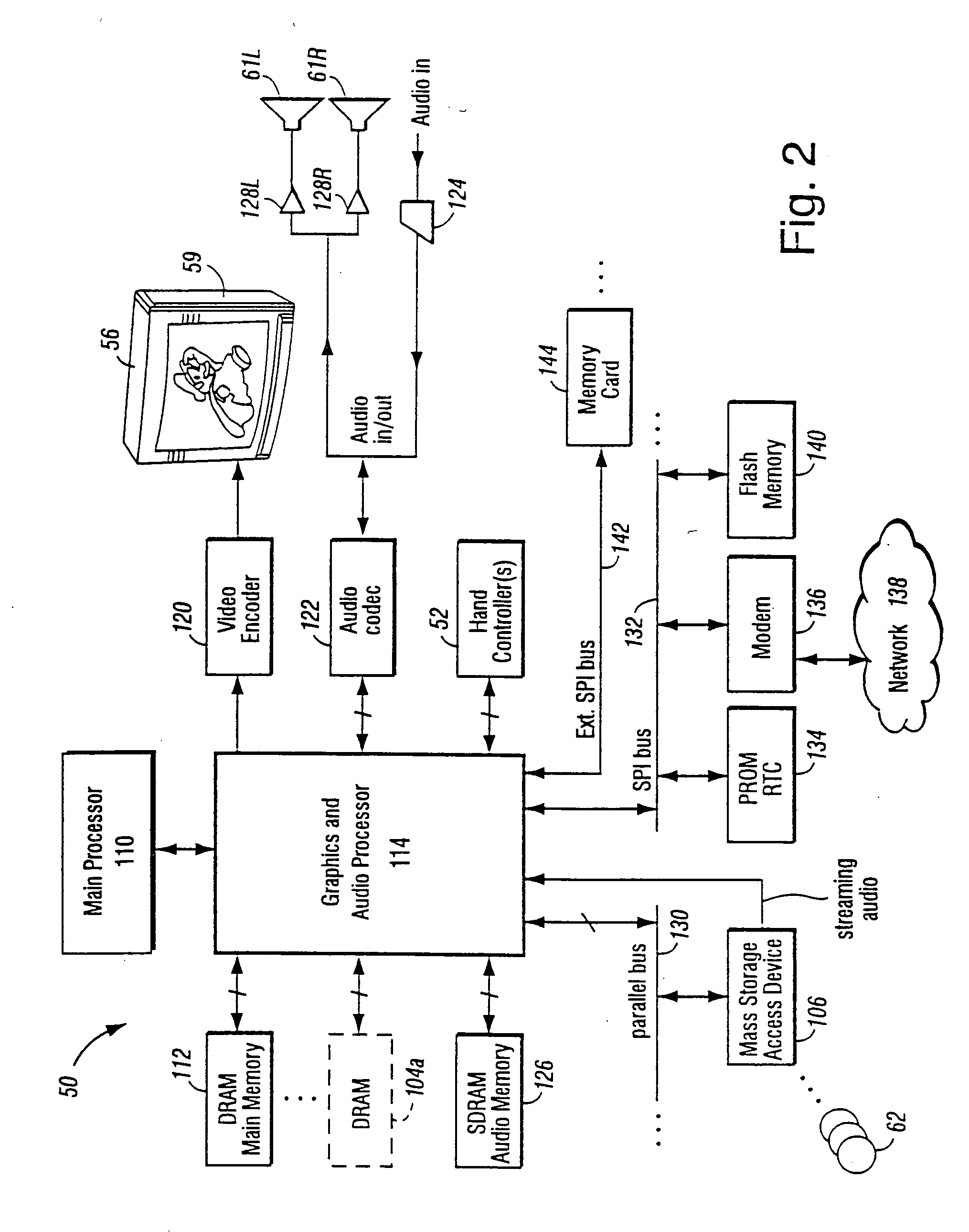
[0088]FIG. 4 shows a more detailed view of an example 3D graphics processor 154. 3D graphics processor 154 includes, among other things, a command processor 200 and a 3D graphics pipeline 180. Main processor 110 communicates streams of data (e.g., graphics command streams and display lists) to command processor 200. Main processor 110 has a two-level cache 115 to minimize memory latency, and also has a write-gathering buffer 111 for uncached data streams targeted for the graphics and audio processor 114. The write-gathering buffer 111 collects partial cache lines into full cache lines and sends the data out to the graphics and audio processor 114 one cache line at a time for maximum bus usage.
[0089] Command processor 200 receives display commands from main processor 110 and parses them—obtaining any additional data necessary to process them from shared memory 112. The command processor 200 provides a stream of vertex commands to graphics pipeline 180 for 2D and / or 3D proces...
example implementation details
[0124] A processor to graphics interface unit portion 202 of the graphics and audio processor 114 command processor 200 contains the control logic for managing the FIFO buffers 210 in main memory 112. FIG. 11 shows an example implementation. In the example shown, all CPU 110 writes to the graphics and audio processor 114 will be routed to the main memory 112. There are two registers that define the portion of the main memory 112 that has been allocated to the graphics FIFO 210 attached to the graphics and audio processor 114:
[0125] the FIFO BASE register 822, and
[0126] the FIFO TOP register 824.
[0127] The FIFO_BASE register 822 defines the base address of the FIFO 210. The FIFO_TOP register 824 defines the last address in the FIFO.
[0128] Command processor 200 keeps track of the read and write pointers for FIFO 210 in hardware. Since all data written into the FIFO are cache line sized, there is no need to keep track of valid bytes. The write pointer 808 is incremented by 32 bytes...
PUM
 Abstract
Description
Claims
Application Information


