Method and device for wavelength-sensitive photo-sensing

a wavelength-sensitive and photo-sensing technology, applied in the field of photo-sensing, can solve the problems of limiting the minimum size of each sensing unit, unable to detect different components simultaneously, and light is absorbed in photoelectric processes

Inactive Publication Date: 2007-07-26
NANYANG TECH UNIV
View PDF7 Cites 60 Cited by
  • Summary
  • Abstract
  • Description
  • Claims
  • Application Information

AI Technical Summary

Problems solved by technology

Secondly, light is absorbed in photoelectric processes as it interacts with, and loses energy to, electrons in its path.
However, this technique has a disadvantage—it cannot detect different components simultaneously.
This requirement limits the minimum size of each sensing unit and thus the spatial resolution of the sensor.

Method used


Image

  • Method and device for wavelength-sensitive photo-sensing
  • Method and device for wavelength-sensitive photo-sensing
  • Method and device for wavelength-sensitive photo-sensing

Examples


Embodiment Construction

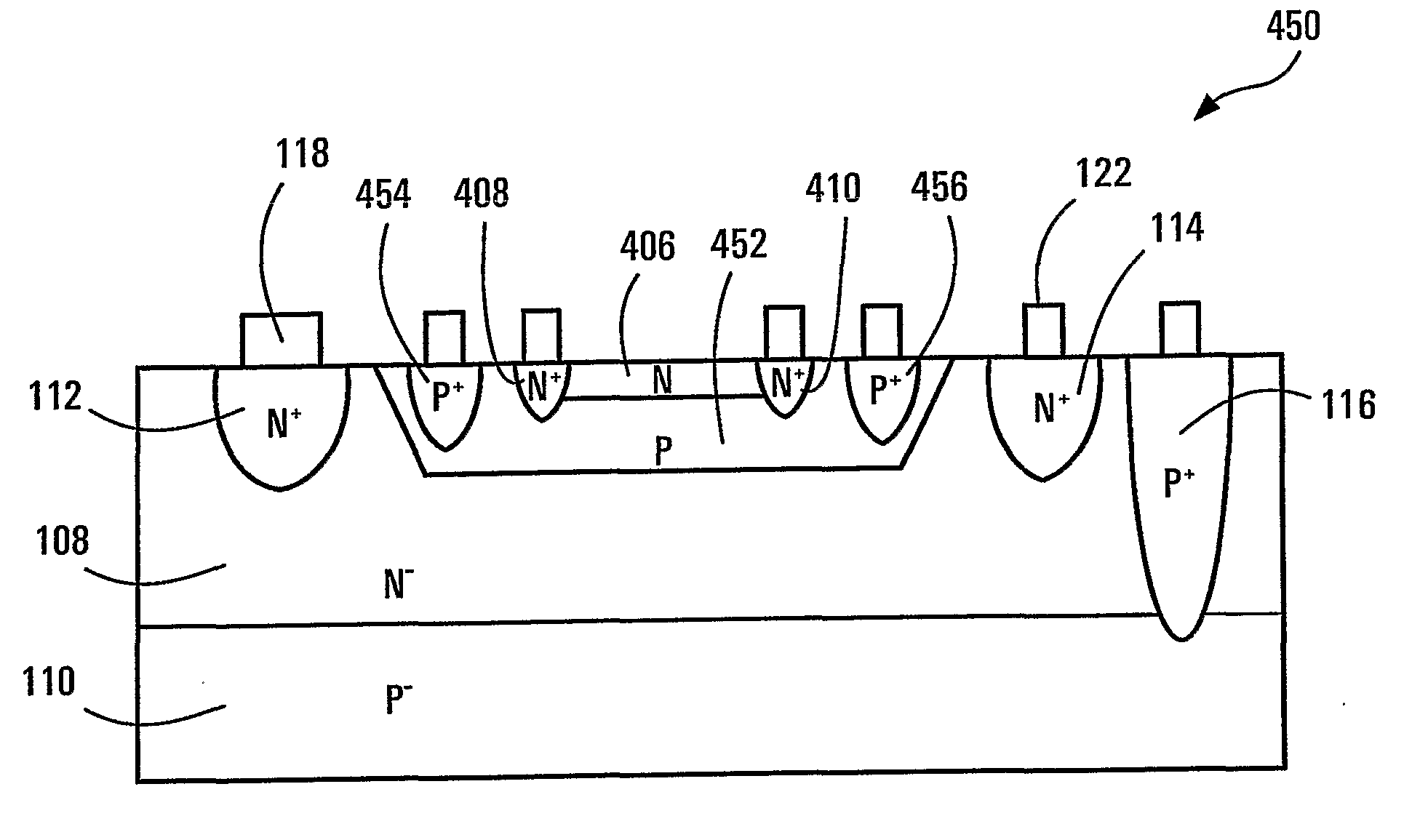
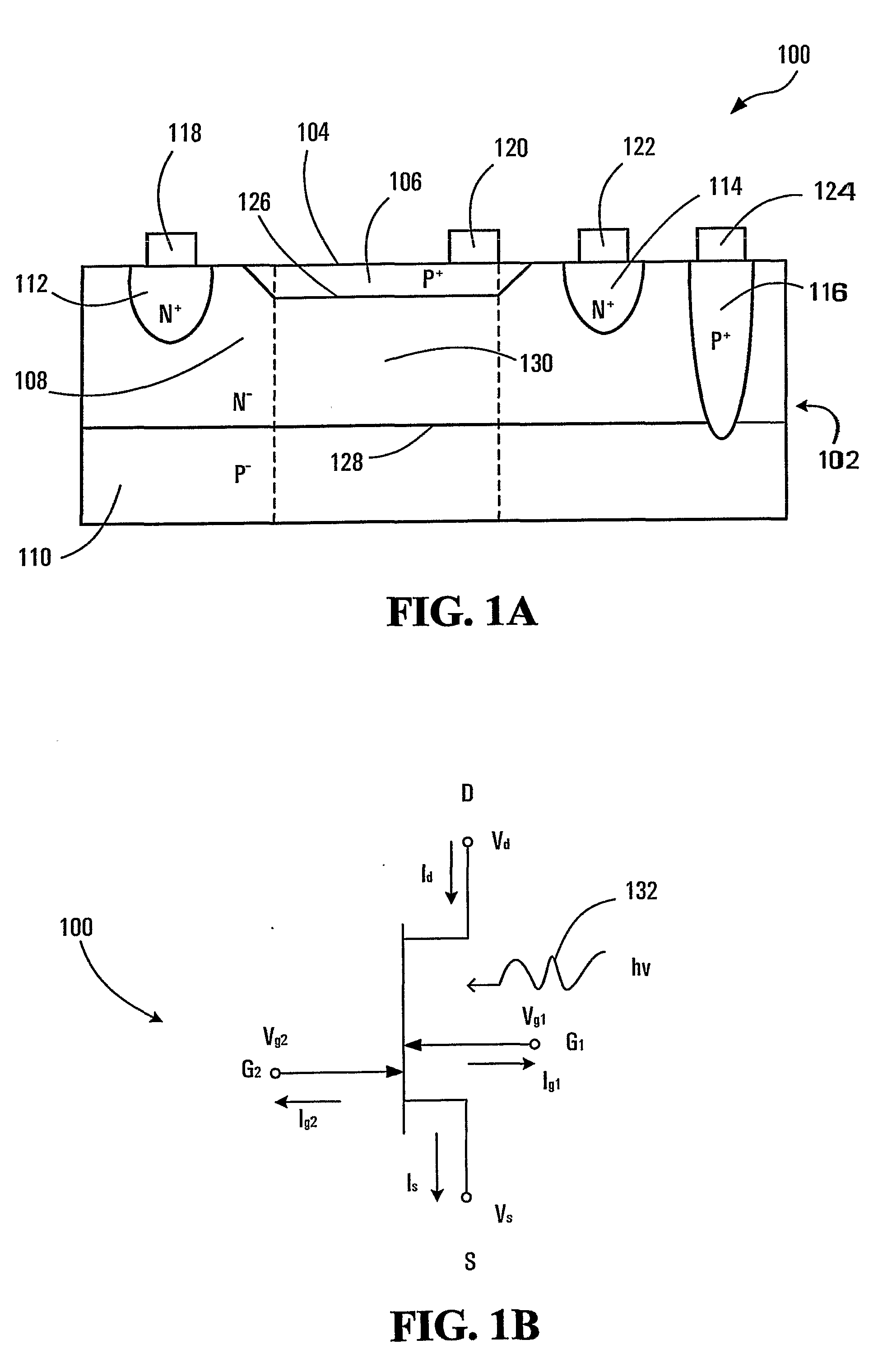
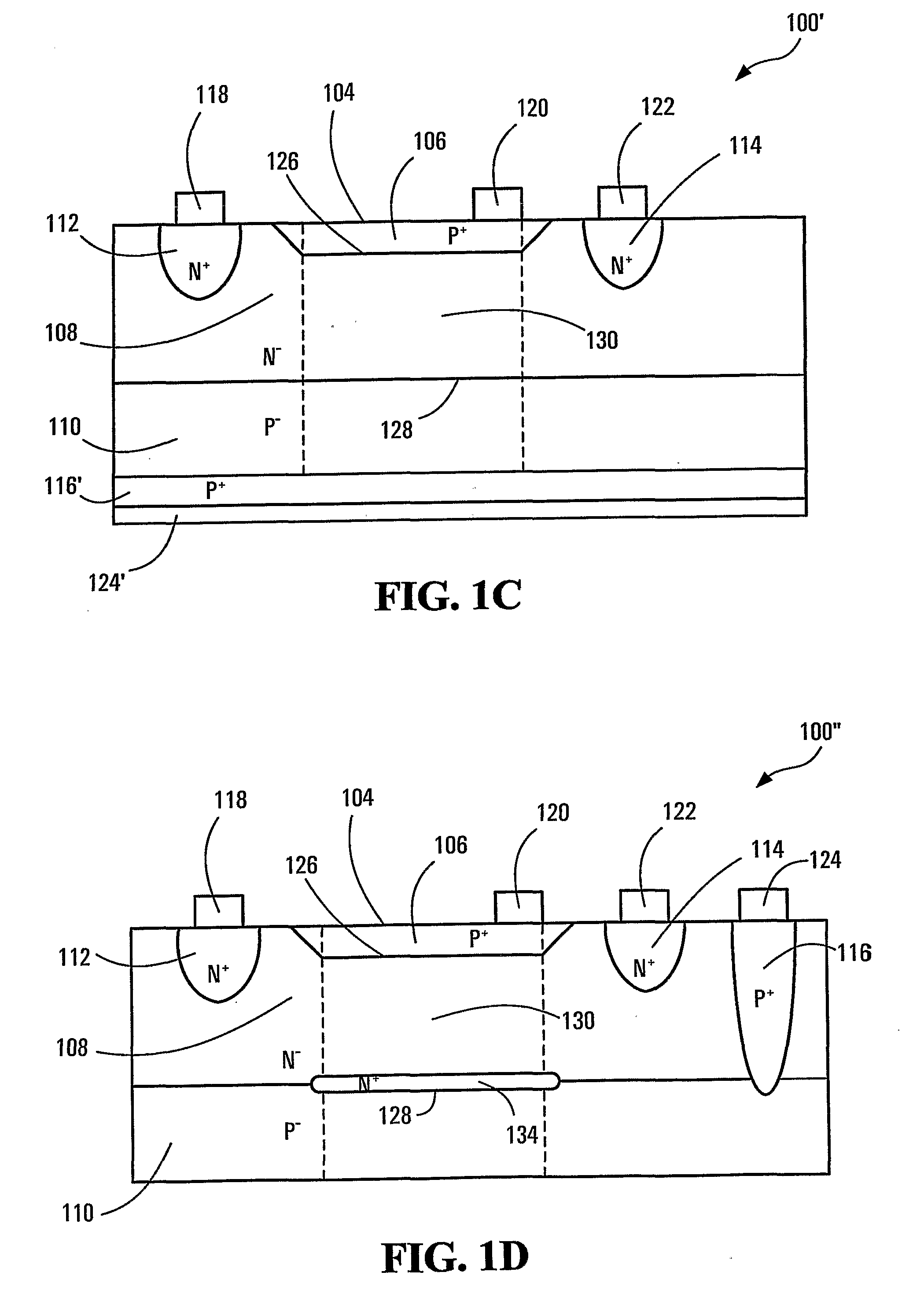
[0035] Color sensing based on pn-junctions takes advantage of the photoelectric effect and the generation of free carriers by light absorption in depletion regions developed around the pn-junctions. The carriers can be collected and detected by sensing a current across each pn-junction.

[0036] Another property of semiconductors that can also be utilized for sensing light is photo-conductivity. Many semiconductors exhibit photo-conductivity. As can be understood, the conductance of a conductive path in a photo-conductive semiconductor can be affected by the absorption of light therein because of the free carriers generated due to photoelectric effect. The conductance can increase when light is absorbed. Within a limit, the higher the light absorption, the higher the conductance. Since light absorption is wavelength dependent, the photo-conductivity of a conductive path has a particular spectral response. A conductive path at a particular depth in a semiconductor is more sensitive to ...


PUM


Abstract

A semiconductor device includes a conducting channel (130) formed beneath a substrate surface with a pre-determined photo-conductivity spectral response. The channel is formed between two pn-junctions (126, 128) defining first and third photo-electric depletion regions at respective depths relative to the surface corresponding to penetration depths of light of different wavelengths. The first region (106) which has the light absorbing surface (104) above the first pn-junction (126) is specific to a first colour. The channel region (130) between the two pn-junctions (126, 128) is photo-conductive to a second colour. The third region below the second pn-junction (128) is sensitive to a third colour. Electrical contacts (118, 120, 122, 124) are disposed on the source (112), the top gate (106), the drain (114) and the bottom gate (116) for receiving the electrical currents induced by the presence of the absorbed wavelengths.

Description

CROSS-REFERENCE TO RELATED APPLICATIONS [0001] This application claims priority from U.S. provisional application No. 60 / 544,496, entitled “COLOR SENSORS BASED ON J(FET) STRUCTURES” and filed Feb. 17, 2004, which is incorporated herein by reference.FIELD OF THE INVENTION [0002] The present invention relates generally to photo-sensing, and more particularly to methods and devices for wavelength-sensitive photo-sensing. BACKGROUND OF THE INVENTION [0003] Wavelength-sensitive photo-sensing (often referred to as color sensing) has applications in a wide range of fields such as medicine and biology, the food, printing, and cosmetics industries, and the like. For example, in the study of cells and tissues, it may be necessary to monitor or detect the transmission and absorption of light of a certain bandwidth by cells and tissues under study. [0004] Semiconductor-based color sensors are known. These sensors typically operate based on the differential absorption of visible light in a solid...

Claims


Application Information

Patent Timeline
Patent Type & Authority Applications(United States)
IPC IPC(8): H01L31/06H01L21/331G01J3/46H01L27/146H01L31/0224
CPCH01L31/1884Y02E10/50H01L31/022408H01L27/14632H01L27/14647H01L27/14603
Inventor POENAR, DANIEL PULUCARP, MIHAELA
Owner NANYANG TECH UNIV
Why Eureka
Try Eureka