Surface acoustic wave device and method of manufacturing the same

a surface acoustic wave and acoustic wave technology, applied in piezoelectric/electrostrictive/magnetostrictive devices, piezoelectric/electrostriction/magnetostriction machines, electrical equipment, etc., can solve the problem of temperature characteristics, inability to achieve sufficient attenuation on the reception side, and inability to achieve sufficient attenuation. the effect of frequency-characteristic change and excellent electrical characteristics

Inactive Publication Date: 2007-07-26
PANASONIC CORP
View PDF6 Cites 4 Cited by
  • Summary
  • Abstract
  • Description
  • Claims
  • Application Information

AI Technical Summary

Benefits of technology

[0011] The foregoing structure allows obtaining surface acoustic wave devices excellent in electrical characteristics, and yet, narrowing the disperse of frequency characteristics change of the devices, which change is caused by temperature.
[0018] The foregoing method allows manufacturing surface acoustic wave devices excellent in electrical characteristics, and yet, narrowing the disperse of their frequency-characteristics changes caused by temperature.

Problems solved by technology

The conventional surface acoustic wave devices, as discussed above, have problems with temperature characteristics.
), a sufficient attenuated amount cannot be expected on the reception side.
However, this conventional method needs heat treatment in order to obtain bonding strength, and it also requires some special washing.

Method used


Image

  • Surface acoustic wave device and method of manufacturing the same
  • Surface acoustic wave device and method of manufacturing the same
  • Surface acoustic wave device and method of manufacturing the same

Examples


Embodiment Construction

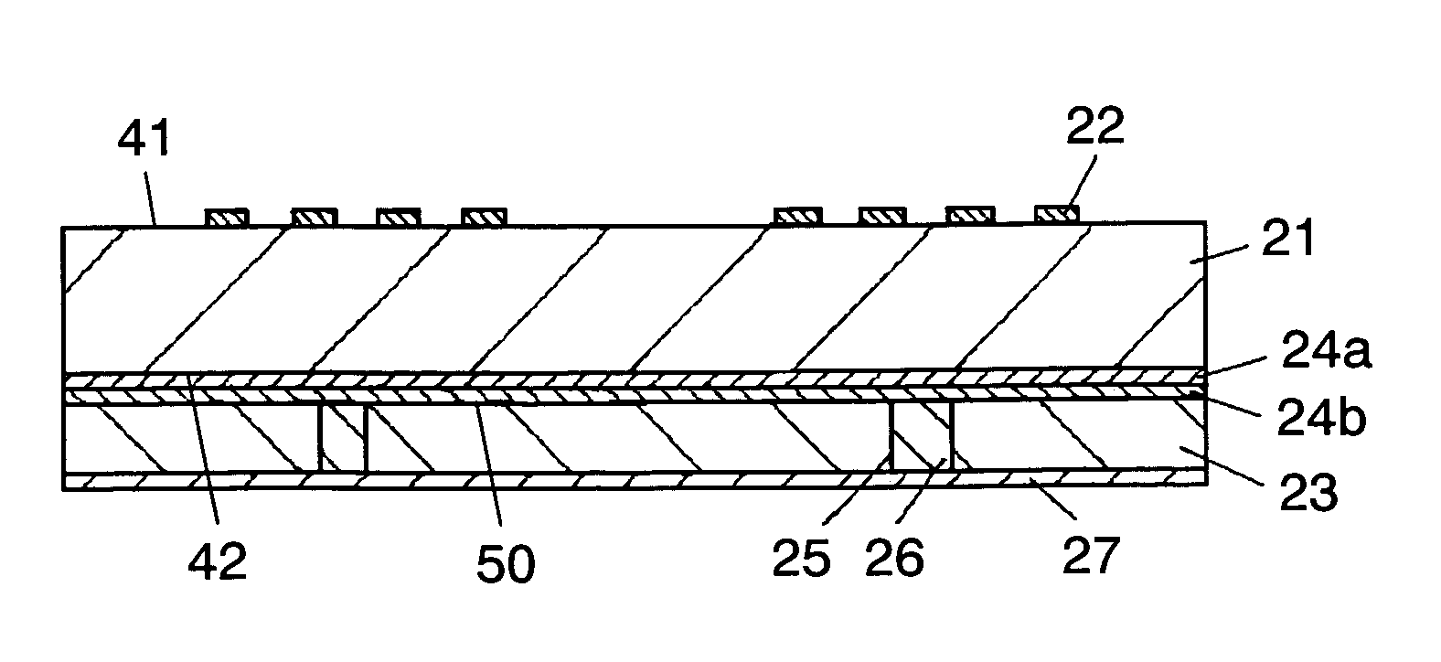
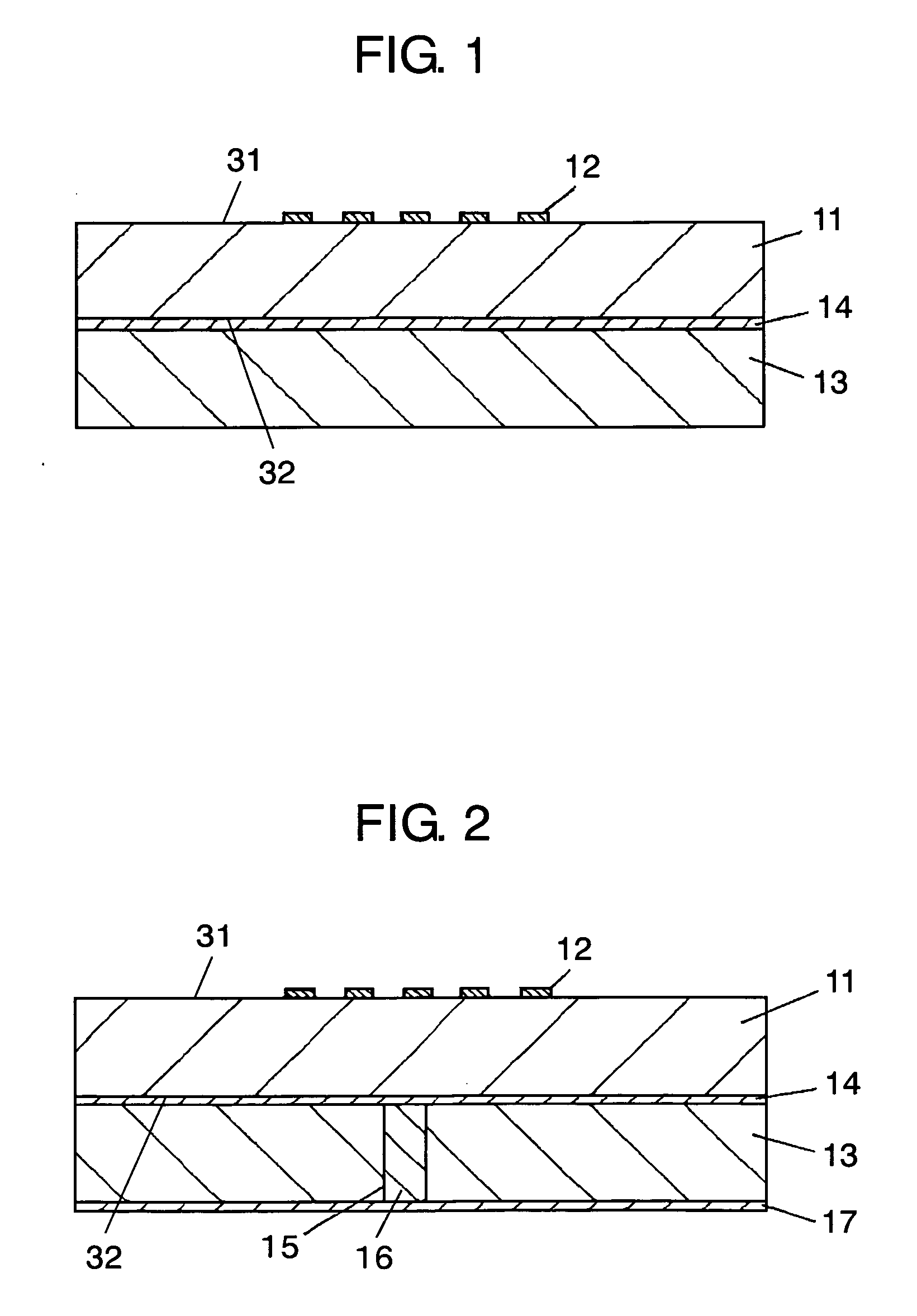
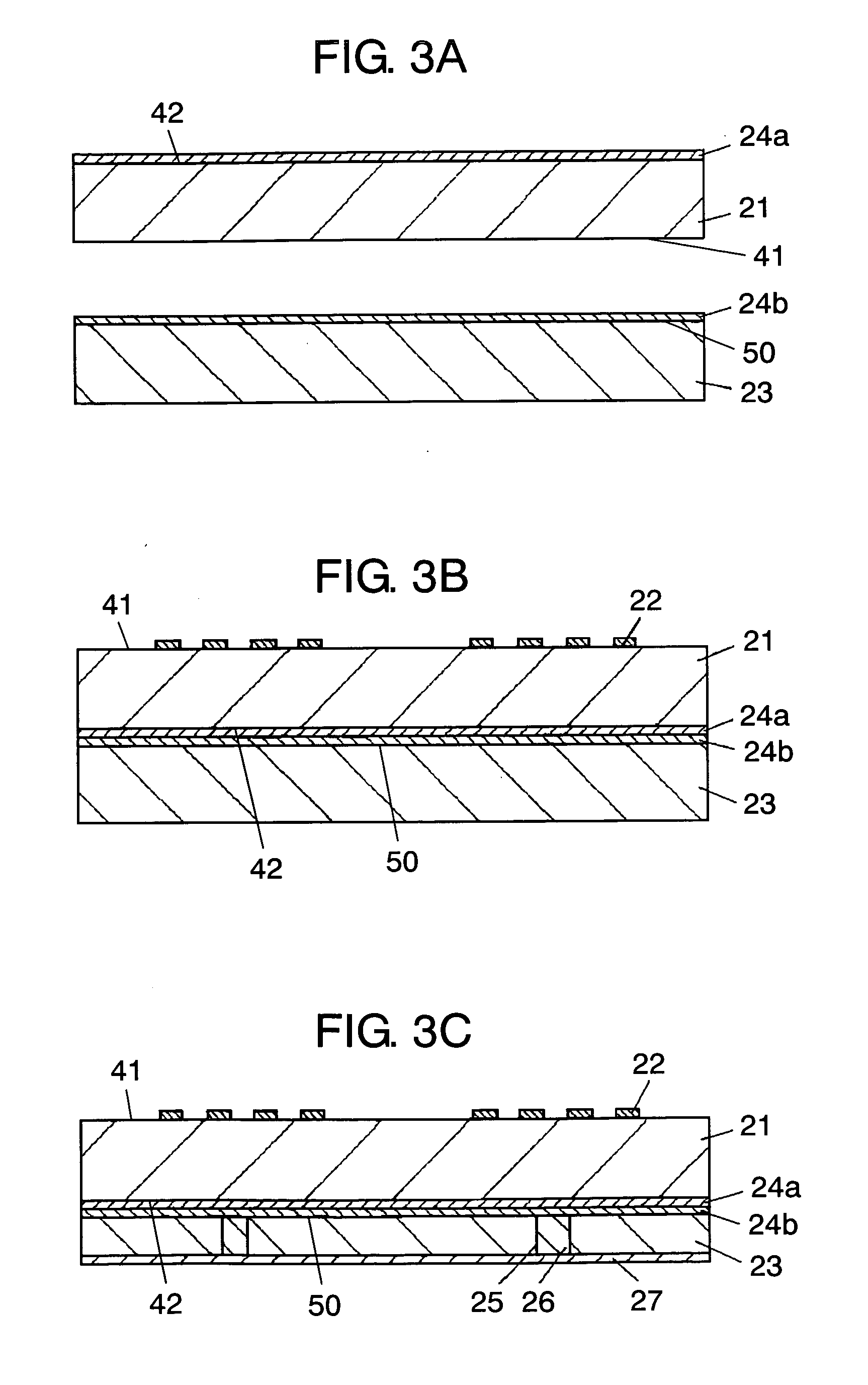
[0036] An exemplary embodiment of the present invention is demonstrated hereinafter with reference to the accompanying drawings. FIG. 1 shows a sectional view of a surface acoustic wave device in accordance with the embodiment of the present invention. The surface acoustic wave device shown in FIG. 1 of the present invention comprises the following element: [0037] piezoelectric substrate 11; [0038] comb-shaped electrode 12 formed on first principal face 31 of piezoelectric substrate 11; and [0039] supporting substrate 13 bonded, via metal layer 14, to second principal face 32 of piezoelectric substrate 11.

[0040] The foregoing surface acoustic wave device is further detailed hereinafter. Piezoelectric substrate 11 is made from rotated Y-cut lithium tantalate, to be more specific, 39° YLT. Comb-shaped electrode 12 is provided onto first principal face 31 of piezoelectric substrate 11. Supporting substrate 13 is made from sapphire or the like. Second principal face 32 of piezoelectric...


PUM


Abstract

A surface acoustic wave device includes a piezoelectric substrate, a comb-shaped electrode formed on a first principal face of the piezoelectric substrate, and a supporting substrate bonded to a second principal face of the piezoelectric substrate. The second principal face of the piezoelectric substrate is bonded to the supporting substrate via a metal layer. A method of manufacturing the surface acoustic wave device includes the steps of: forming a first metal layer on the second principal face of the piezoelectric substrate, forming a second metal layer on a principal face of the supporting substrate, activating the surfaces of the first and second metal layers in plasma atmosphere, bonding the first and second metal layers together at room temperature, and forming the comb-shaped electrode on the first principal face of the piezoelectric substrate.

Description

TECHNICAL FIELD [0001] The present invention relates to surface acoustic wave devices to be used in mobile telephones among others, and it also relates to a method of manufacturing the same devices. BACKGROUND ART [0002] Recently compact and lightweight surface acoustic wave devices have been widely used in electronic apparatuses such as a variety of mobile communication terminals. Among other these devices, surface acoustic wave filters formed of lithium tantalate (hereinafter simply referred to as LT) substrate are widely employed in the radio circuit of mobile telephone systems working in the frequency range between 800 MHz and 2 GHz. The LT substrate often employs an LT substrate having X-axis propagation of surface acoustic wave in 39° Y-cut LT (hereinafter referred to simply as 39° YLT), namely, this LT substrate is cut out from Y-plane at rotating angle of 39° on X-axis toward Z-axis. [0003] However, the 39° YLT substrate has a greater thermal expansion coefficient along the ...

Claims


Application Information

Patent Timeline
Patent Type & Authority Applications(United States)
IPC IPC(8): H03H9/25
CPCH03H3/10H03H9/02834H03H9/02574
Inventor TAKAYAMA, RYOUICHIMATSUI, ATSUSHI
Owner PANASONIC CORP
Why Eureka
Try Eureka