
Organic light emitting display device

a display device and organic technology, applied in the direction of discharge tube luminescnet screens, discharge tube/lamp details, electric discharge lamps, etc., can solve the problems of increasing material and process costs, deteriorating electrical characteristics and/or light-emitting characteristics, and increasing the thickness of the display devi

Active Publication Date: 2007-07-26
SAMSUNG DISPLAY CO LTD
View PDF98 Cites 117 Cited by
  • Summary
  • Abstract
  • Description
  • Claims
  • Application Information

AI Technical Summary

Benefits of technology

The invention provides an organic light-emitting display device and a method of making it. The device includes an array of organic light-emitting pixels formed over a first substrate, and a second substrate placed over the first substrate. A first frit seal is interposed between the first and second substrates, and a second frit seal is interposed between the first and second substrates. The first and second frit seals may form a closed loop around the array. The device may also include a third frit seal and a fourth frit seal. The frit seals may be attached to the substrates with or without materials between them. The device is enclosed and filled with a gas other than air. The method includes interposing the array, interposing the first and second frits, melting and solidifying the frits, and optionally cutting the resulting product. The technical effects of the invention include improved sealing and reduced air entering the device, and improved reliability and performance.

Problems solved by technology

However, since the organic light-emitting device includes organic material, it may be vulnerable to oxygen and since the cathode electrode is made of metal material, it is easily oxidized by moisture in the air to possibly deteriorate its electrical characteristics and / or light-emitting characteristics.
However, the method of mounting the moisture absorbent material in the form of a powder has problems that include such things as manufacturing process complications, material and process cost increases, increased thickness of a display device, and difficulty in applying to a front light-emitting display configuration.
Also, the method of coating or adhering the moisture absorbent in the form of a film has problems in that it is limited in its ability to remove moisture and the adhesive force between the sealant and the substrate may become weakened due to possible outgassing during the curing process, lowering the durability and the reliability of the device.
However, if the laser is not irradiated at a constant power and speed, the frit may be bonded to the substrate in a state where the frit is not completely melted so that the interface adhesive force between the frit and the substrate may be partially weakened.
If the frit is delaminated in the defective portion, it may cause an infiltration of oxygen or moisture.
However, if the laser power is increased, the frit may be cracked by the high heat, or since high heat is transferred to the light-emitting device in a portion adjacent to the frit, the function of the light-emitting device may be lost or degraded.

Method used


Image

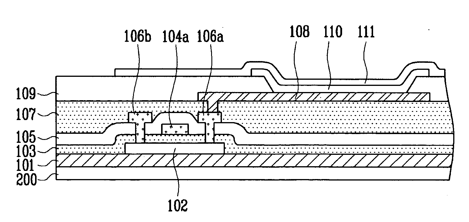
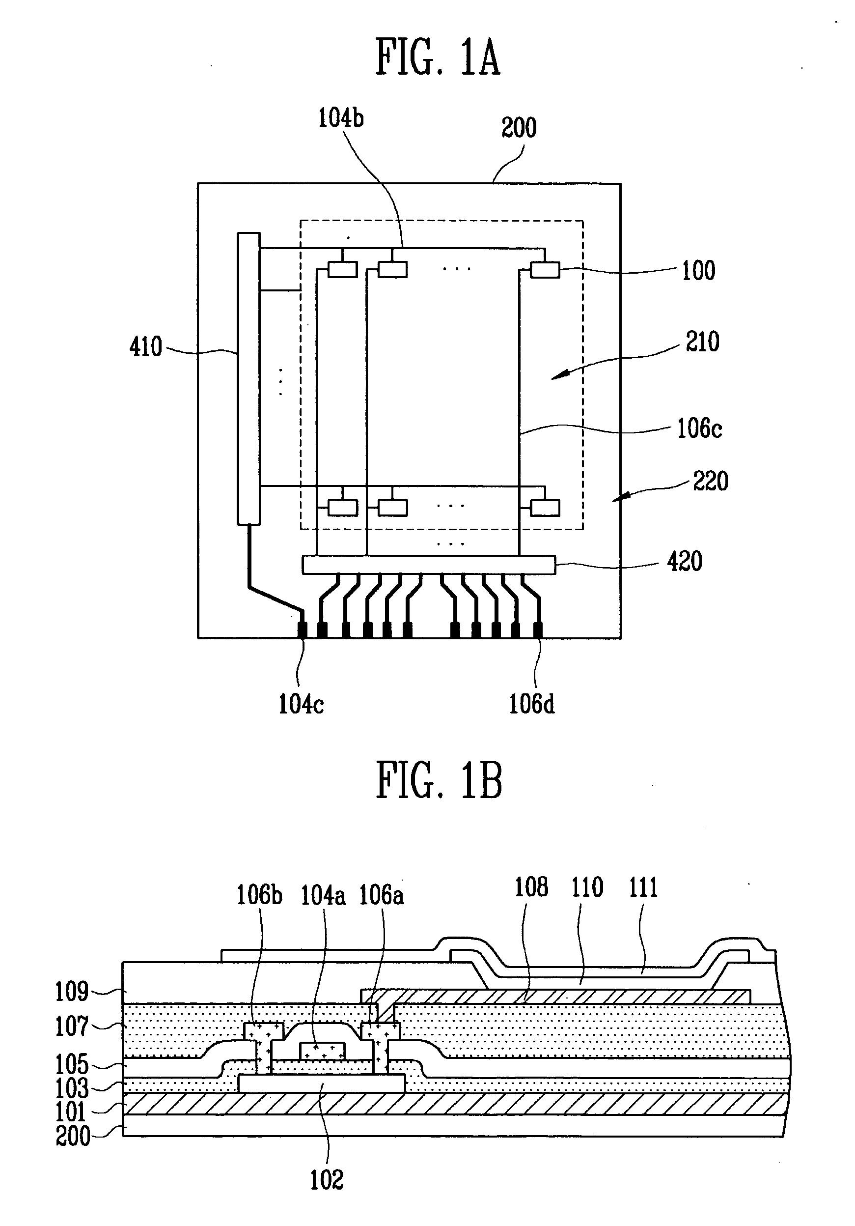
  • Organic light emitting display device
  • Organic light emitting display device
  • Organic light emitting display device

Examples


Embodiment Construction

[0027]Hereinafter, preferable embodiments according to the present invention will be described with reference to the accompanying drawings. Here, when one device is connected to another device, one device may be not only directly connected to another device but also indirectly connected to another device via another device. Further, irrelevant devices are omitted for clarity. Also, like reference numerals refer to like devices throughout.

[0028]An organic light emitting display (OLED) is a display device comprising an array of organic light emitting diodes. Organic light emitting diodes are solid state devices which include an organic material and are adapted to generate and emit light when appropriate electrical potentials are applied.

[0029]OLEDs can be generally grouped into two basic types dependent on the arrangement with which the stimulating electrical current is provided. FIG. 4A schematically illustrates an exploded view of a simplified structure of a passive matrix type OLED...


PUM


Abstract

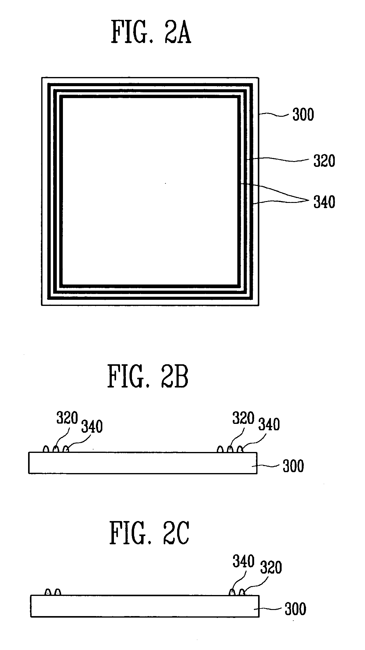
Disclosed is an organic light-emitting display device comprising: a pixel region wherein an organic light-emitting device comprised of a first electrode, an organic thin film layer and a second electrode is formed; a first substrate comprising a non-pixel region encompassing the pixel region; a second substrate disposed on the upper of the first substrate to be overlapped with the pixel region and a portion of the non-pixel region; and a plurality of frits provided between the first substrate and the second substrate and formed in parallel at spaced intervals along the peripheral portion of the pixel region, wherein the first substrate is bonded to the second substrate by the plurality of frits. Even in the case that a portion of the frit is delaminated due to a partial defection thereof, its encapsulation state can be maintained as it is by being encapsulated with the frit in a multi structure and even in the case that a substrate with a large diameter is used, the width and height of the frit do not need to increase.

Description

CROSS-REFERENCE TO RELATED APPLICATIONS[0001]This application claims the benefit of Korean Patent Application No. 2006-8463, filed on Jan. 26, 2006, in the Korean Intellectual Property Office, the disclosure of which is incorporated herein by reference in its entirety. This application is related to and incorporates herein by reference the entire contents of the following concurrently filed applications:ApplicationTitleAtty. Docket No.Filing DateNo.ORGANIC LIGHT-EMITTING DISPLAYSDISHN.043AUSDEVICE AND METHOD OFFABRICATING THE SAMEORGANIC LIGHT-EMITTING DISPLAYSDISHN.045AUSDEVICE AND METHOD OFMANUFACTURING THE SAMEORGANIC LIGHT-EMITTING DISPLAYSDISHN.051AUSDEVICE WITH FRIT SEAL ANDREINFORCING STRUCTUREORGANIC LIGHT EMITTING DISPLAYSDISHN.052AUSDEVICE METHOD OF FABRICATINGTHE SAMEORGANIC LIGHT EMITTING DISPLAYSDISHN.053AUSAND METHOD OF FABRICATING THESAMEORGANIC LIGHT-EMITTING DISPLAYSDISHN.054AUSDEVICE WITH FRIT SEAL ANDREINFORCING STRUCTURE BONDEDTO FRAMEMETHOD FOR PACKAGING ORGANIC...

Claims


Application Information

Patent Timeline
Patent Type & Authority Applications(United States)
IPC IPC(8): H01J1/62H01J63/04
CPCH01L51/5246H10K59/8722A47G25/1421H10K50/8426
Inventor CHOI, DONG SOOPARK, JIN WOO
Owner SAMSUNG DISPLAY CO LTD
Learn More