Unlock instant, AI-driven research and patent intelligence for your innovation.

Semiconductor integrated circuit

a technology of integrated circuits and semiconductors, applied in logic circuits, logic circuit coupling/interface arrangements, pulse techniques, etc., can solve the problems of total operation speed or power consumption, factor of deterioration in performance, etc., and achieve the effect of reducing power consumption and power consumption of semiconductor integrated circuits

Inactive Publication Date: 2007-07-26
SOCIONEXT INC
View PDF10 Cites 4 Cited by
  • Summary
  • Abstract
  • Description
  • Claims
  • Application Information

AI Technical Summary

Benefits of technology

[0009] It is an object of the invention to realize a semiconductor integrated circuit with a less power consumption by reducing a power consumption due to a signal line of a large load.
[0011] Since the driver circuit driving the signal line is provided with the first p-type transistor and the second n-type transistor, the amplitude of the signal to be transmitted via the signal line can be reduced to an amplitude from a potential higher than the potential of the low power supply line by an absolute value of a threshold voltage of the first p-type transistor to a potential lower than the potential of the high power supply line by a threshold voltage of the first n-type transistor. As a result, it is possible to reduce the power consumption due to the signal line. This can greatly contribute to reduction of power consumption of the semiconductor integrated circuit, in case that a load of the signal line to be driven by the driver circuit is large.
[0014] The driver circuit driving the signal line is provided with the first p-type transistor and the second p-type transistor, so that the amplitude of the signal to be transmitted via the signal line can be reduced to an amplitude from a potential higher than the potential of the low power supply line by an absolute value of a threshold voltage of the first p-type transistor to the potential of the high power supply line. As a result, it is possible to reduce the power consumption due to the signal line. This can greatly contribute to reduction of power consumption of the semiconductor integrated circuit, in case that a load of the signal line to be driven by the driver circuit is large.
[0016] Since the positive-phase side driver circuit driving the positive-phase side signal line is provided with the positive-phase side first p-type transistor and the positive-phase side second p-type transistor, the amplitude of the signal to be transmitted via the positive-phase side signal line can be reduced to an amplitude from a potential higher than the potential of the low power supply line by an absolute value of a threshold voltage of the positive-phase side first p-type transistor to the potential of the high power supply line. Similarly, the negative-phase side driver circuit driving the negative-phase side signal line is provided with the negative-phase side first p-type transistor and the negative-phase side second p-type transistor, the amplitude of the signal to be transmitted via the negative-phase side signal line can be reduced to an amplitude from a potential higher than the potential of the low power supply line by an absolute value of a threshold voltage of the negative-phase side first p-type transistor to the potential of the high power supply line. As a result, it is possible to reduce the power consumption due to the positive-phase side signal line and the negative-phase side signal line. This can greatly contribute to reduction of the power consumption of the semiconductor integrated circuit, in case that loads of the positive-phase side signal line and the negative-phase side signal line to be driven by the positive-phase side driver circuit and the negative-phase side driver circuit respectively are large.
[0018] Since the driver circuit driving the signal line is provided with the first n-type transistor and the second n-type transistor, the amplitude of the signal to be transmitted via the signal line can be reduced to an amplitude from the potential of the low power supply line to a potential lower than the potential of the high power supply line by a threshold voltage of the first n-type transistor. As a result, it is possible to reduce the power consumption due to the signal line. This can greatly contribute to reduction of the power consumption of the semiconductor integrated circuit, in case that a load of the signal line to be driven by the driver circuit is large.
[0020] Since the positive-phase side driver circuit driving the positive-phase side signal line is provided with the positive-phase side first n-type transistor and the positive-phase side second n-type transistor, the amplitude of the signal to be transmitted via the positive-phase side signal line can be reduced to an amplitude from a potential of the low power supply line to a potential lower than the potential of the high power supply line by a threshold voltage of the positive-phase side first n-type transistor. Similarly, the negative-phase side driver circuit driving the negative-phase side signal line is provided with the negative-phase side first n-type transistor and the negative-phase side second n-type transistor, so that the amplitude of the signal to be transmitted via the negative-phase side signal line can be reduced to an amplitude from the potential of the low power supply line to the potential lower by a threshold voltage of the negative-phase side first n-type transistor than the potential of the high power supply line. As a result, it is possible to reduce the power consumption due to the positive-phase side signal line and the negative-phase side signal line. This can greatly contribute to reduction of the power consumption of the semiconductor integrated circuit, in case that loads of the positive-phase side signal line and the negative-phase side signal line to be driven by the positive-phase side driver circuit and the negative-phase side driver circuit respectively are large.

Problems solved by technology

In the semiconductor integrated circuit constituted of a plurality of circuit blocks, the wiring lengths of inter-block signal lines (e.g., global signal lines) for transmitting signals between the circuit blocks have been increasing, causing one of major factors to deteriorate the performances (e.g., the operation speed or the power consumption) of the semiconductor integrated circuit.
In recent years, the power consumption due to a signal line of a long wiring length (e.g., a signal line of a large load) such as an inter-block signal line has largely accounted for the total power consumption of the semiconductor integrated circuit.

Method used


Image

  • Semiconductor integrated circuit
  • Semiconductor integrated circuit
  • Semiconductor integrated circuit

Examples


first embodiment

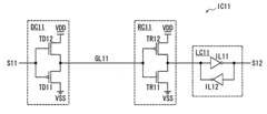
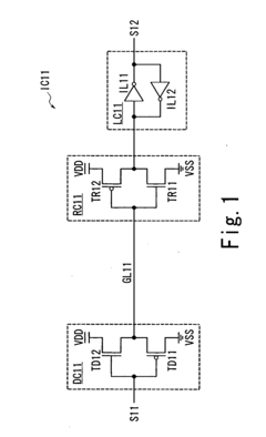
[0039] Embodiments of the invention are described with reference to the accompanying drawings. FIG. 1 shows the invention. A semiconductor integrated circuit IC11 includes: a signal line GL11; a driver circuit DC11 for driving the signal line GL11 in accordance with an input signal S11; a receiver circuit RC11 for generating an output signal in accordance with the potential of the signal line GL11; and a latch circuit LC11 for latching the output signal of the receiver circuit RC11 to generate an output signal S12. For example, the driver circuit DC11 and the receiver circuit RC11 are disposed in different circuit blocks arranged at a spacing. The latch circuit LC11 is disposed in the same circuit block as that of the receiver circuit RC11. The signal line GL11 is the so-called global signal line (e.g., an inter-block signal line) and has a large load.

[0040] The driver circuit DC11 includes a pMOS transistor TD11 (e.g., a first p-type transistor) and an nMOS transistor TD12 (e.g., a...

second embodiment

[0052]FIG. 5 shows the operation waveforms of the invention. When the input signal S11 transits from the ground potential VSS to the power supply potential VDD (FIG. 5(a)), only the nMOS transistor TD12 is turned ON to raise the potential of the signal line GL11 (FIG. 5(b)). When the potential of the signal line GL11 is raised to the intermediate potential VMH, the nMOS transistor TD12 is turned OFF. When the control signal CTL transits in this state from the ground potential VSS to the power supply potential VDD (FIG. 5(c)), the nMOS transistor TR13 and the pMOS transistor TR14 are turned ON so that the output signal of the receiver circuit RC12 transits from the power supply potential VDD to the ground potential VSS. As a result, the output signal S12 of the latch circuit LC11 transits from the ground potential VSS to the power supply potential VDD (FIG. 5(d)). When the control signal CTL transits from the power supply potential VDD to the ground potential VSS (FIG. 5(e)), the nMO...

fifth embodiment

[0063]FIG. 8 shows the invention. A semiconductor integrated circuit IC21 is configured to include: a signal line GL21; a driver circuit DC21 for driving the signal line GL21 in accordance with an input signal S21; a receiver circuit RC21 for generating an output signal in accordance with the potential of the signal line GL21; and a latch circuit LC21 for latching the output signal of the receiver circuit RC21 to generate an output signal S22. For example, the driver circuit DC21 and the receiver circuit RC21 are disposed in different circuit blocks arranged at a spacing. The latch circuit LC21 is disposed in the same circuit block as that of the receiver circuit RC21. The signal line GL21 is a global signal line of a large load.

[0064] The driver circuit DC21 is configured to include a pMOS transistor TD21 (e.g., a first p-type transistor), a pMOS transistor TD22 (e.g., a second p-type transistor) and an inverter ID21. The pMOS transistor TD21 has its source connected with the signa...


PUM


Abstract

A driver circuit for a signal line of a large load is configured to include: a pMOS transistor having a source and a drain connected with a signal line and a ground line, respectively, and a gate receiving an input signal; and an nMOS transistor having a source and a drain connected with a signal line and a power supply line, respectively, and a gate receiving the input signal. As a result, the power consumption due to the signal line of a large load is reduced to realize a reduction of the power consumption of a semiconductor integrated circuit.

Description

CROSS REFERENCE TO RELATED APPLICATION [0001] This application is based upon and claims the benefit of priority from Japanese Patent Application No. 2006-004569, filed on Jan. 12, 2006, the entire contents of which are incorporated herein by reference. BACKGROUND OF THE INVENTION [0002] 1. Field of the Invention [0003] The present invention relates to a semiconductor integrated circuit and, more particularly, to a technique for reducing the power consumption of a semiconductor integrated circuit. [0004] 2. Description of the Related Art [0005] Recently, mobile electronic devices (e.g., a mobile telephone) driven by a battery have been commonly used. There have been a strong demand for a semiconductor integrated circuit to be mounted on those mobile electronic devices to have a high-speed operation in order to achieve the advanced functions of the electronic devices and to have a low power consumption for enabling the battery to run for a long time. [0006] In the semiconductor integr...

Claims


Application Information

Patent Timeline
IPC IPC(8): H03K19/094
CPCH03K19/018571
Inventor AKIYOSHI, HIDEO
Owner SOCIONEXT INC