Flat display structure and method for driving flat display

a flat display and display structure technology, applied in the field of flat display and driving method thereof, can solve the problems of gate signal distortion and gate delay, affecting largely display quality, and achieve the effect of improving display quality and reducing gate delay and signal distortion

Active Publication Date: 2007-07-26
AU OPTRONICS CORP
View PDF2 Cites 39 Cited by
  • Summary
  • Abstract
  • Description
  • Claims
  • Application Information

AI Technical Summary

Benefits of technology

[0011] It is therefore an object of the invention to provide a flat display structure and method for driving a flat display. After each gate line outputs a gate signal to turn on the corresponding pixel row, the driving circuit of the flat display turns on each voltage adapting device, which is coupled to the gate line and disposed on the substrate, to output a working voltage of the driving circuit to the corresponding gate line and promptly adjusts the gate signal to a predetermined level. Consequently, gate delay and signal distortion are decreased without affecting the aperture ratio, hence largely improving the display quality.

Problems solved by technology

In a conventional large-scaled glass on array (GOA) liquid crystal display (LCD), the gate line has a high loading charge, so the gate signal is likely to be coupled with the clock signal of the driving circuit, resulting in the problems of gate signal distortion and gate delay.
However, within the display time of one frame, each of the NMOS transistors Q1˜Qn is only turned on once and is incapable of decreasing the ripples generated when the NMOS transistor is not turned on, largely affecting the display quality.

Method used


Image

  • Flat display structure and method for driving flat display
  • Flat display structure and method for driving flat display
  • Flat display structure and method for driving flat display

Examples


first embodiment

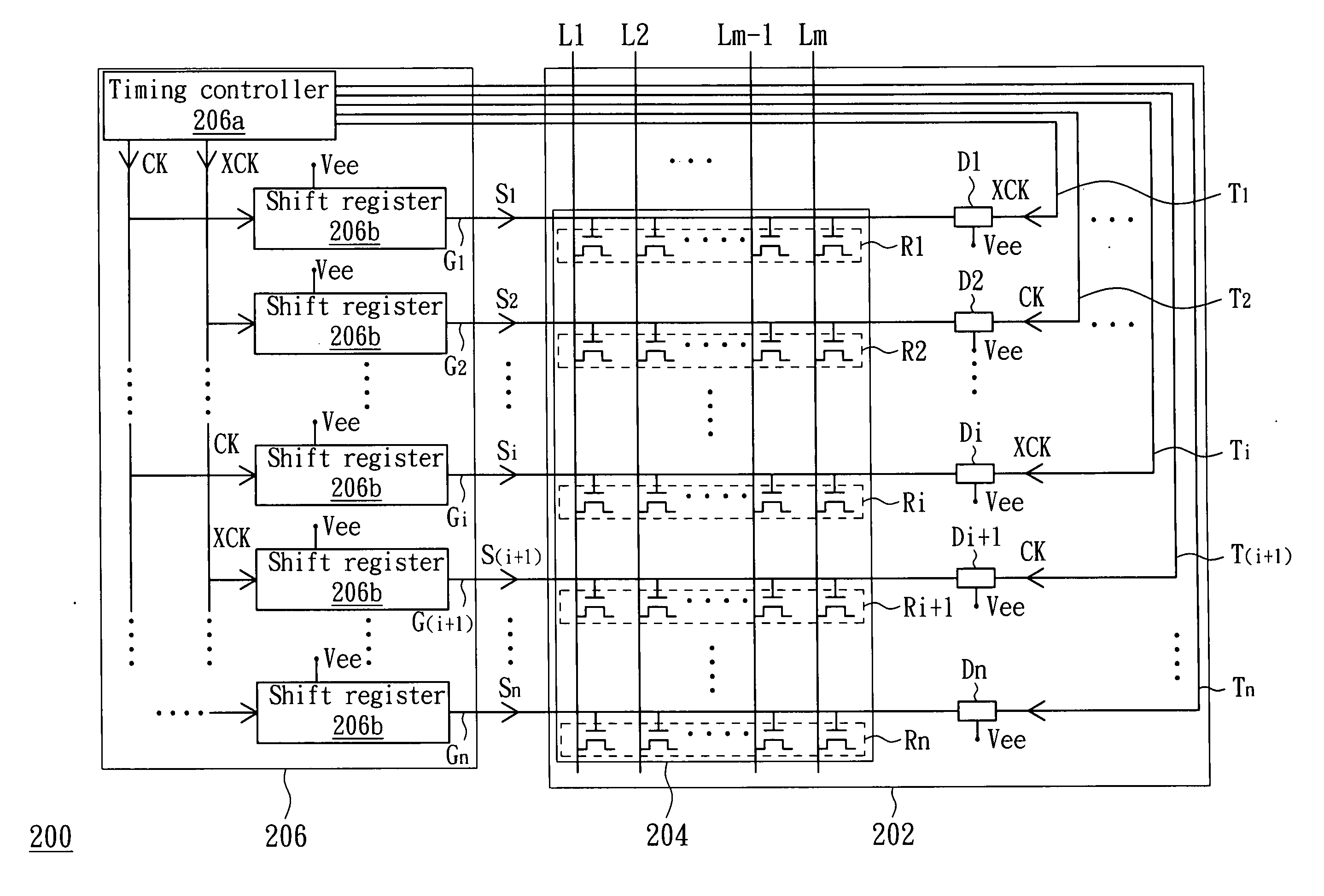
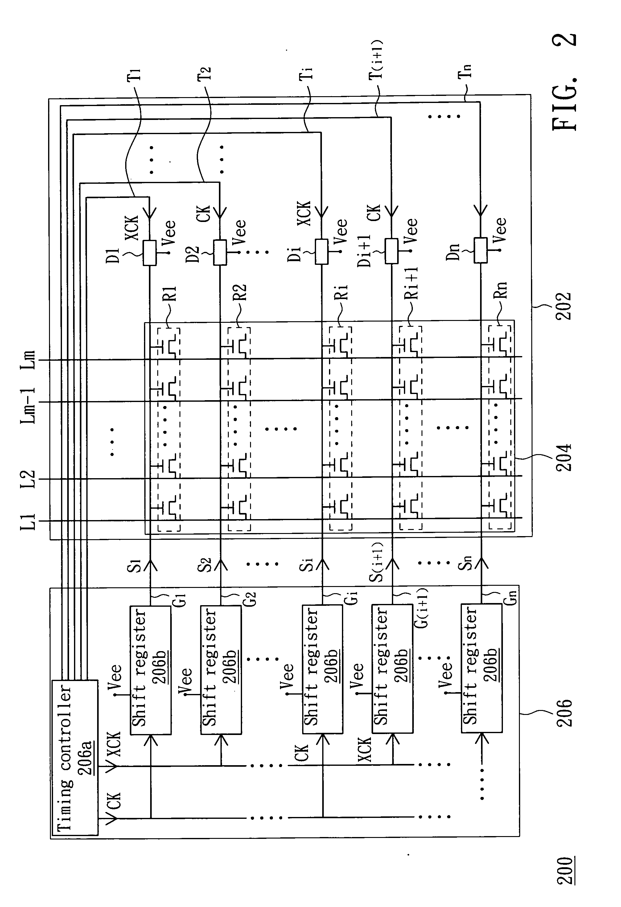
[0025] Referring to FIG. 2, the circuit structure of a flat display according to a first embodiment of the invention is sown. Examples of the flat display 200 includes a substrate 202, gate lines G1˜Gn, data lines L1˜Lm, a driving circuit 206 and n voltage adapting devices Dj (j=1˜n), wherein n is a positive integer. As shown in FIG. 2, the gate lines G1˜Gn and the data lines L1˜Lm are disposed on the substrate 202 and together form a pixel matrix 204 which includes n pixel rows Ri, i=1˜n.

[0026] The driving circuit 206 further includes a timing controller 206a and n shift registers 206b. The n shift registers 206b sequentially outputs gate signals S1˜Sn through the gate lines G1˜Gn to enable each pixel row Ri according to the clock signals CK and XCK outputted by the timing controller 206a. The phase of the XCK signal is reverse to the phase of the CK signal.

[0027] As shown in FIG. 2, the first transmission lines T1˜Tn are disposed on some area of the substrate 202 other than the ...

second embodiment

[0036] The second embodiment differs with the first embodiment in that the driving circuit 206 further outputs a number of second control signals such as the clock signal XCK or CK to the voltage adapting devices D1˜Dn through second transmission lines T1′˜Tn′ disposed on some area of the substrate 202 other than the pixel matrix 204. The voltage adapting device Di is coupled to the corresponding second transmission line Ti.

[0037] Referring to FIG. 5, the structure of a voltage adapting device Di according to a second embodiment of the invention is shown. The flat display structure in the present invention discussed herein means layouts or circuits within the flat panel. As shown in FIG. 5, the voltage adapting device Di includes NMOS transistors M1, M2, M3 and M4. The drain of the NMOS transistor M2 is coupled to the corresponding gate line Gi, and the source of the NMOS transistor M2 is coupled to the working voltage Vee. The drain of the NMOS transistor M3 is coupled to the seco...


PUM


Abstract

A flat display structure including a substrate, a pixel matrix, a driving circuit and several voltage adapting devices and driving method thereof are provided. Each of voltage adapting devices includes an input terminal, a first control terminal and an output terminal. The input terminal is electrically connected to the i-th gate line Gi corresponding to the i-th pixel row Ri. The first control terminal is adapted to receive a first control signal. The output terminal is adapted to receive a working voltage.

Description

[0001] This application claims the benefit of Taiwan application Serial No. 95103162, filed Jan. 26, 2006, the subject matter of which is incorporated herein by reference. BACKGROUND OF THE INVENTION [0002] 1. Field of the Invention [0003] The invention relates in general to a flat display and driving method thereof, and more particularly to a flat display structure using a voltage adapting device to input a working voltage to a gate line and driving method thereof. [0004] 2. Description of the Related Art [0005] In a conventional large-scaled glass on array (GOA) liquid crystal display (LCD), the gate line has a high loading charge, so the gate signal is likely to be coupled with the clock signal of the driving circuit, resulting in the problems of gate signal distortion and gate delay. To resolve the coupling and distortion problems, a pull down circuit is disposed on each gate line to improve the display quality. [0006] Referring to FIG. 1, partial structure of a conventional GOA...

Claims


Application Information

Patent Timeline
Patent Type & Authority Applications(United States)
IPC IPC(8): G09G3/36
CPCG02F1/13454G09G3/3648G09G2320/0252G09G2300/0426G09G3/3677
Inventor CHANG, LEE-HSUNLIN, YU-WENLI, CHUNG-LUNGCHENG, YUNG-TSE
Owner AU OPTRONICS CORP
Why Eureka
Try Eureka