Memory circuit including a resistive memory element and method for operating such a memory circuit

a memory circuit and resistive memory technology, applied in the direction of information storage, static storage, digital storage, etc., can solve the problems of resistive memory element resistive memory element,

Active Publication Date: 2007-07-26
INFINEON TECH AG
View PDF15 Cites 65 Cited by
  • Summary
  • Abstract
  • Description
  • Claims
  • Application Information

AI Technical Summary

Benefits of technology

[0006] It is therefore an object of the present invention to provide a memory circuit and a method for operating such a memory circ

Problems solved by technology

As the changing of the resistance of the resistive memory element during the programming from the high resistance state to the low resistance state is quite short, the current through the resistive memory element results in a charging the parasitic capacity of the bit

Method used


Image

  • Memory circuit including a resistive memory element and method for operating such a memory circuit
  • Memory circuit including a resistive memory element and method for operating such a memory circuit
  • Memory circuit including a resistive memory element and method for operating such a memory circuit

Examples


first embodiment

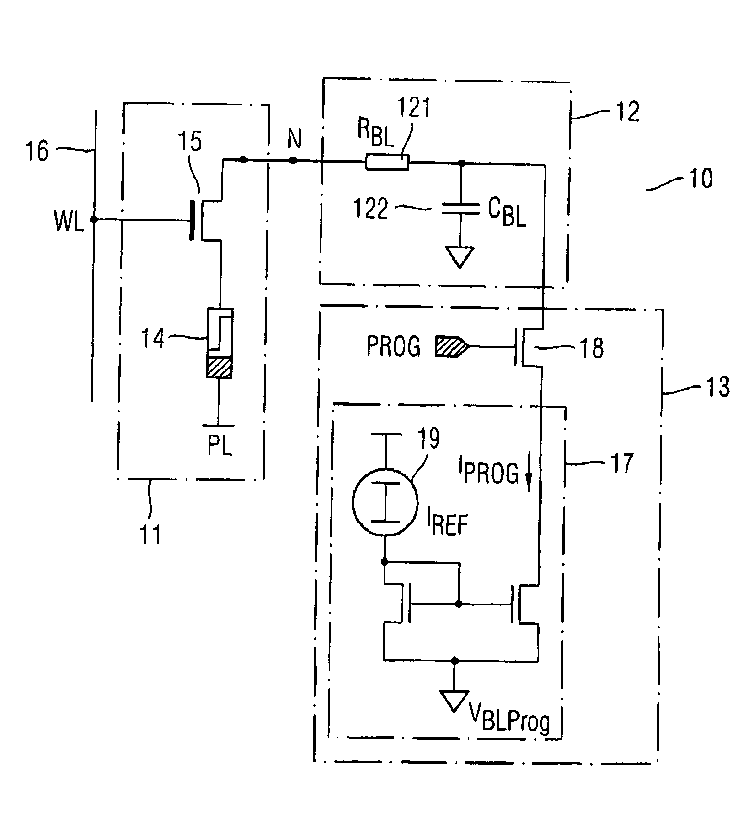
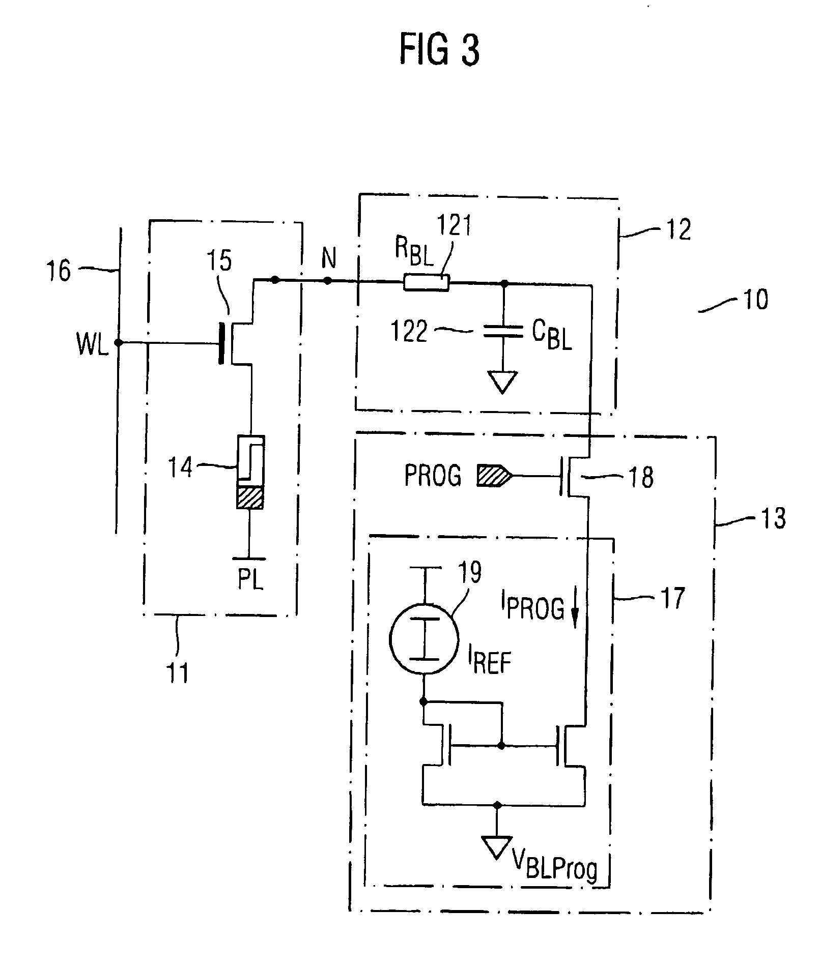
[0049] In FIG. 5, a memory circuit according to the present invention is depicted. In the following embodiments, the same reference signs indicate same elements or elements having a similar function. A bleeder circuit 20 is provided and connectable to the bit line 12 close to the resistive memory cell 11, close to the programming circuit 13 or close to any other position of the bit line. In the given examples the bleeder circuit 20 is located close to the node N which is located along the bit line 12. Furthermore, a data line (not shown) may be provided to which the programming circuit 13 is coupled wherein with the data line the bit lines are connected directly or via respective addressing switches, e.g. in form of column-select-transistors.

[0050] To avoid any further influences of the bleeder circuit 20 onto the operation of the memory circuit 10, the bleeder circuit is applied to the bit line 12 merely during the time the cell current through the resistive memory element 14 excee...

second embodiment

[0051] In FIG. 6, the present invention is shown wherein the bleeder circuit 20 is illustrated in more detail. The bleeder circuit 20 comprises a bleeder transistor 21 which is coupled to a bleeder potential VBLEED, preferably the plate potential, by a first terminal and with the bit line 12 by a second terminal. A gate terminal of the bleeder transistor 21 is coupled to a control circuit 22 which controls the bleeder transistor 21 to couple or decouple the bleeder potential VBLEED with the bit line 12. Instead of the plate potential, any other appropriate potential can be used which supports the potential change resulting from the rapid change of the resistance of the resistive memory element 14 on the bit line 12. The control circuit 22 closes the bleeder transistor 21 at the time when the resistance change of the resistive memory element 14 occurs and preferably opens the bleeder transistor 21 when the cell current through the resistive memory element 14 equals or has approached ...

third embodiment

[0052] In FIG. 7, the present invention is illustrated. In order to switch the bleeder circuit 20 on to a specific time, a comparator 25 can be used. The comparator receives a reference voltage VREF which is preferably set to the programming voltage at a first input. A second input of the comparator 25 is connected to the bit line 12 to receive the bit line potential. The comparator 25 is operable to detect the appliance of the programming potential wherein the comparator 25 closes the bleeder transistor 21 such that a higher current can be supplied to the bit line 12 as long as the potential of the bit line 12 has not reached the programming potential. The reference voltage VREF can be set such that the bleeder transistor 21 closes when the bit line potential exceeds the programming potential far more than a threshold voltage and remains closed until the bit line potential has approached the programming potential for less than a threshold voltage. Thereby, the time period during wh...


PUM


Abstract

The present invention relates to a memory circuit and method of operating the same. In at least one embodiment, the memory circuit includes a resistive memory element coupled to a plate potential by a first terminal; a bit line which is connectable to a second terminal of the resistive memory element; a programming circuit operable to change the resistance of the resistive memory element; a bleeder circuit operable to provide a bleeding current to or from the bit line due to a change of the resistance of the resistive memory element caused by the programming circuit.

Description

BACKGROUND OF THE INVENTION [0001] 1. Field of the Invention [0002] The present invention relates to a memory circuit including a resistive memory element such as a CBRAM memory element, also called a PMC element (PMC: programmable metallization cell). The present invention further relates to a method for operating such a memory circuit. [0003] 2. Description of the Related Art [0004] A CBRAM memory element, which in the following shall be called resistive memory element, comprises a dielectric material in which a conductive path can be established and degenerated. By applying electrical field, ions from a conductive material of an electrode move into the dielectric material and form the conductive path. By applying a reversed electrical field, the ions of the conductive material are removed from the dielectric material back towards the electrode in such a way that the resistive memory element is rendered non-conductive. In other words, the resistive memory element can have differen...

Claims


Application Information

Patent Timeline
IPC IPC(8): G11C11/00
CPCG11C13/0011G11C13/004G11C13/0069G11C2213/79G11C2013/0078G11C2013/009G11C2013/0054
Inventor HOENIGSCHMID, HEINZDIMITROVA, MILENALIAW, CORVINANGERBAUER, MICHAEL
Owner INFINEON TECH AG
Why Eureka
Try Eureka