Semiconductor memory device adapted to communicate decoding signals in a word line direction

Active Publication Date: 2007-07-26
SAMSUNG ELECTRONICS CO LTD
View PDF22 Cites 0 Cited by
  • Summary
  • Abstract
  • Description
  • Claims
  • Application Information

AI Technical Summary

Benefits of technology

[0016]Embodiments of the invention provide a semiconductor memory device in which each decoding

Problems solved by technology

In particular, when delay decoding signals PXD1> and PXD2> are driven to a high voltage level of boost voltage level VPP, the relatively heavy load caused by delay decoding signals PXB1> and PXB2>

Method used


Image

  • Semiconductor memory device adapted to communicate decoding signals in a word line direction
  • Semiconductor memory device adapted to communicate decoding signals in a word line direction
  • Semiconductor memory device adapted to communicate decoding signals in a word line direction

Examples


Example

[0030]Embodiments of the invention will be described with reference to the accompanying drawings.

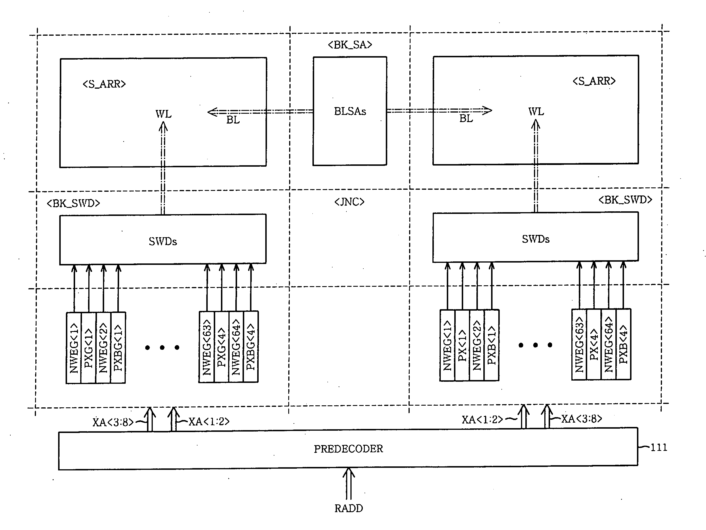
[0031]FIG. 3 is a diagram illustrating the layout of a semiconductor memory device in accordance with an embodiment of the invention. For purposes of clarity, elements illustrated in FIG. 3 are not drawn to scale.

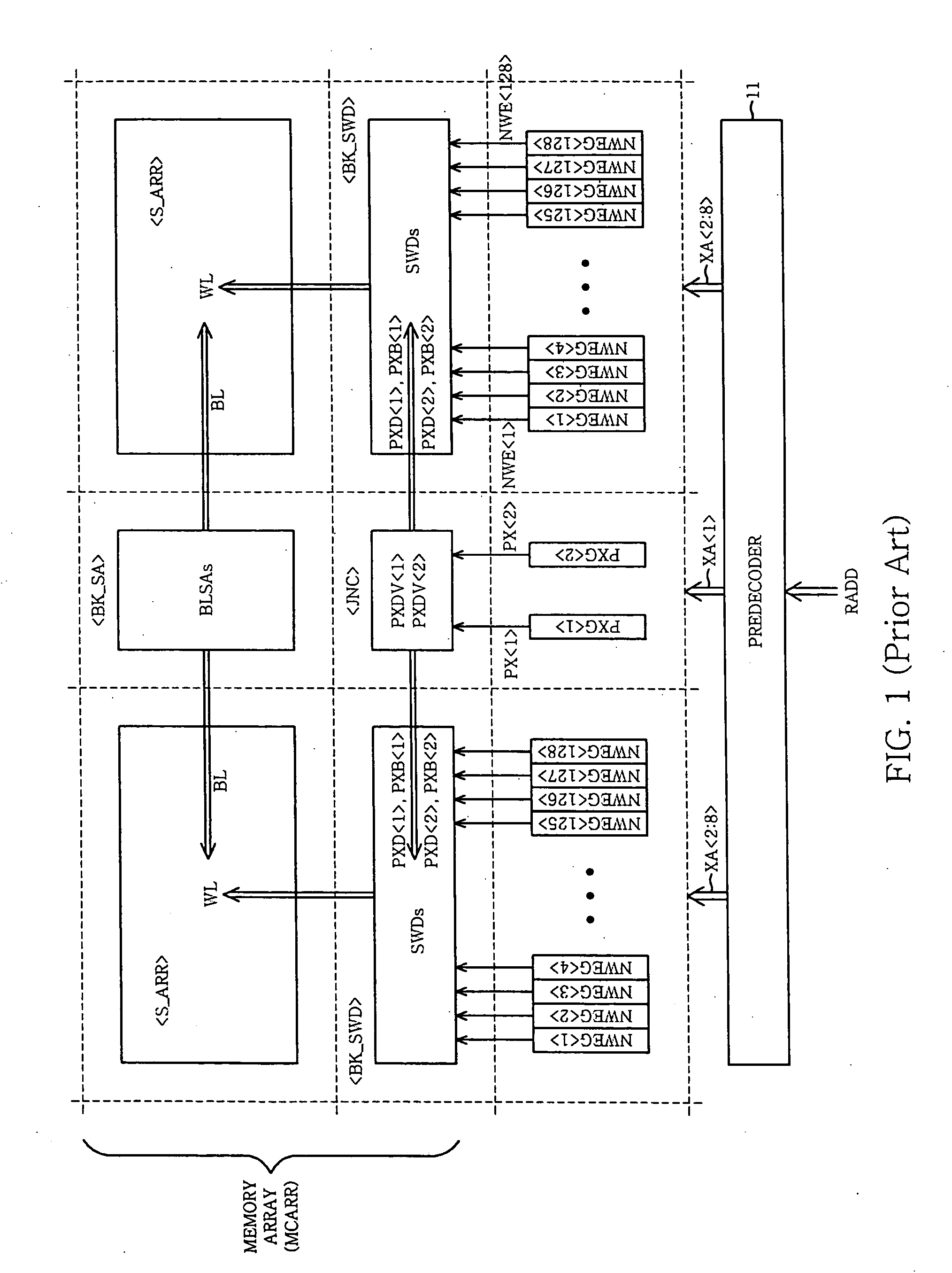
[0032]The semiconductor memory device of the embodiment illustrated in FIG. 3 comprises a plurality of sub-arrays S_ARRs, a plurality of sense amplifier areas BK_SAs (though only one is shown in FIG. 3), and a plurality of word line driver areas BK_SWDs.

[0033]Each of the plurality of sub-arrays S_ARRs comprises a plurality of word lines WLs, a plurality of bit lines BLs and / BLs, and a plurality of memory cells MCs. Two neighboring bit lines BL and / BL constitute a pair of bit lines. Furthermore, each memory cell MC of the plurality of memory cells MCs is disposed at the intersection of one of the word lines WLs and one of the pairs of bit lines BLs and / BLs.

[0034]Each of sense ...


PUM


Abstract

A semiconductor memory device comprising decoding signals communicated solely in a word line direction is provided. The semiconductor memory device comprises a sub-array comprising a plurality of memory cells, a plurality of enable signal generators adapted to generate word line enable signals, a plurality of decoding signal generators adapted to generate decoding signals, a plurality of inverted decoding signal generators adapted to generate inverted decoding signals, and a word line driver area comprising a plurality of sub-word line drivers. Each sub-word line driver is adapted to drive a word line in accordance with one of the word line enable signals and a pair of first signals comprising one of the decoding signals and one of the inverted decoding signals. The word line enable signals and the decoding signals are communicated to the sub-word line drivers solely in a word line direction.

Description

BACKGROUND[0001]1. Field of the Invention[0002]Embodiments of the invention relate to a semiconductor memory device. More particularly, embodiments of the invention relate to a semiconductor memory device including decoding signal generators adapted to generate decoding signals.[0003]This application claims priority to Korean Patent Application No. 10-2006-6052, filed on Jan. 20, 2006, the subject matter of which is hereby incorporated by reference in its entirety.[0004]2. Description of Related Art[0005]A conventional semiconductor memory device includes a memory array including memory cells (which are storage elements capable of storing data) disposed in a matrix having rows and columns. In the conventional semiconductor memory device illustrated in FIG. (FIG.) 1, word lines WLs are disposed along the rows of the matrix (i.e., in a row direction), and bit lines BLs are disposed along columns of the matrix (i.e., in a column direction). Memory cells MCs are respectively disposed at...

Claims


Application Information

Patent Timeline
IPC IPC(8): G11C8/00
CPCG11C8/10G09B21/00G10C3/12G10C9/00G10H2220/221G10H2230/005
Inventor KIM, DOO YOUNG
Owner SAMSUNG ELECTRONICS CO LTD
Why Eureka
Try Eureka