Electron source substrate and image-forming apparatus

Inactive Publication Date: 2005-09-15
CANON KK
View PDF3 Cites 2 Cited by
  • Summary
  • Abstract
  • Description
  • Claims
  • Application Information

AI Technical Summary

Benefits of technology

[0010] The invention is made in consideration of the foregoing conventional problems and it is an object of the invention to provide an electron source substrate which can suppress a leakage current flowing across device electrodes at the time of a

Problems solved by technology

Hitherto, with respect to an electron source substrate in which an electron-emitting device comprising a pair of device electrodes and an electroconductive thin film which is formed over the device electrodes and has an electron-emitting region is formed on an insulative substrate, when the surface of the substrate is charged, electron-emitting characteristics of the electron-emitting device become unstable and a discharge deterioration of the electron-emitting device is caused.
Therefore, such a situation that a thickness of antistatic film near the electron-emitting device increases due to a delicate balance of thicknesses of the device electrodes, the electroconductive thin film, the X-directional wirings, and the Y-dir

Method used


Image

  • Electron source substrate and image-forming apparatus
  • Electron source substrate and image-forming apparatus
  • Electron source substrate and image-forming apparatus

Examples


embodiment 1

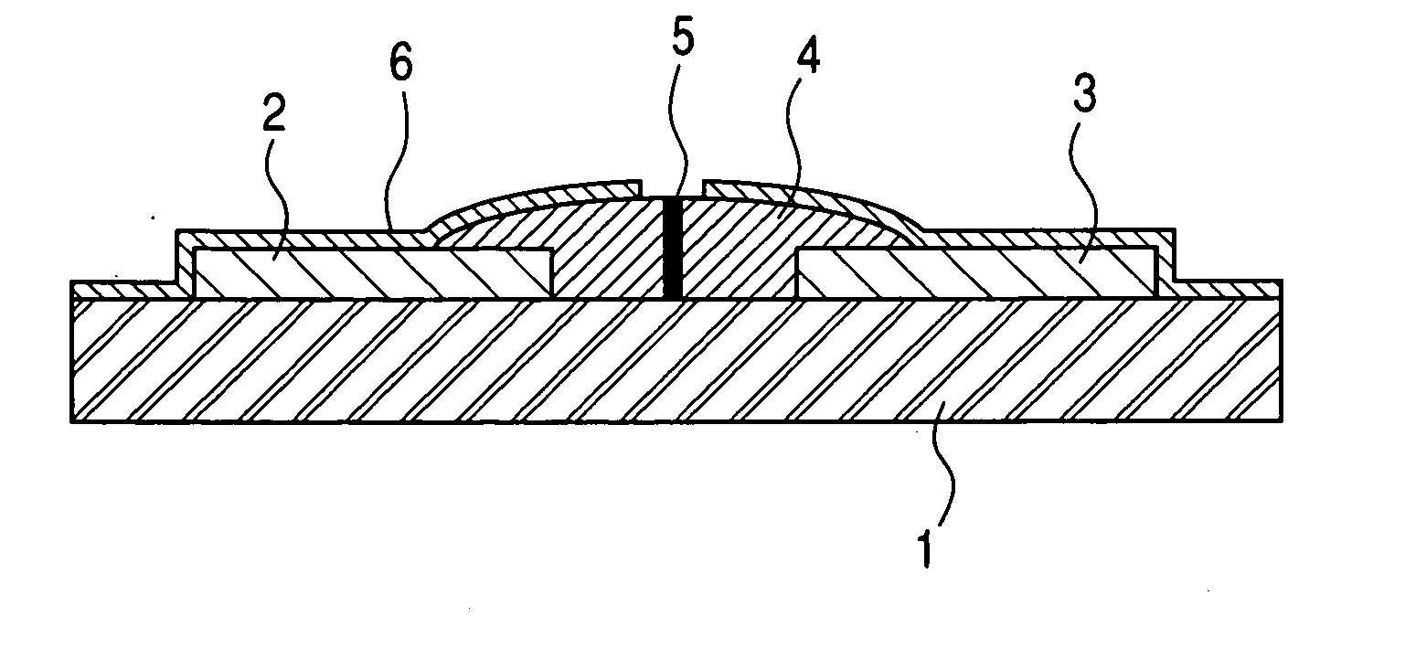
[0082] With respect to the substrate 1 shown in FIG. 8 obtained until the electroconductive thin film 4 is formed after the device electrodes 2 and 3 were formed as mentioned above, the creation, forming, and activation of the antistatic film 6, which will be. explained hereinbelow, are executed and characteristics are evaluated.

(Creation of the Antistatic Film)

[0083]FIG. 9 is a schematic plan view showing a fundamental construction regarding the pair of device electrodes 2 and 3 on the substrate 1 shown in FIG. 8 which is obtained until the electroconductive thin film 4 is formed after the device electrodes 2 and 3 were formed as mentioned above. The whole surface of the substrate 1 in the state of FIG. 9 is coated with a photosensitive resist liquid. As shown in FIG. 10, the electroconductive thin film 4 is divided into almost halves and patterned so that a resist film 100 remains only on the side of one of the device electrodes 2 and 3 (device electrode 3 side in FIG. 10). The...

embodiment 2

[0105] In a manner similar to the embodiment 1, with respect to the substrate 1 shown in FIG. 8 and obtained until the electroconductive thin film 4 is formed after the device electrodes 2 and 3 were formed, the whole surface of the substrate 1 on which the device electrodes 2 and 3 and the like have been formed is coated with a coating liquid of an antistatic film similar to that in the embodiment 1 by a spray coating method similar to that in the embodiment 1 (however, the resist films 100 and 130 are not provided), baked in the atmospheric baking furnace at 350 to 400° C. for 10 to 30 minutes, thereby forming the antistatic film 6 (refer to FIGS. 1 and 2).

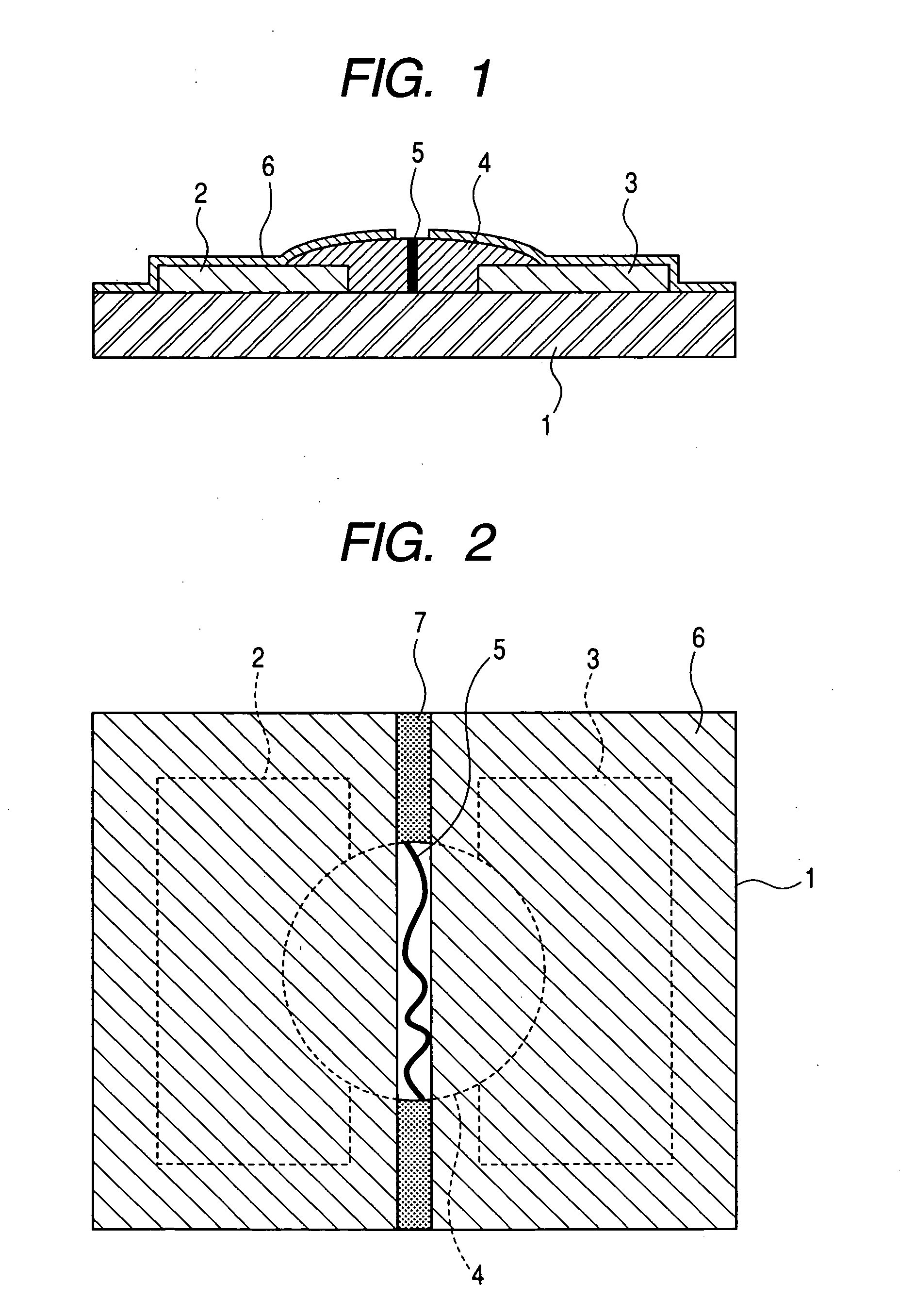
[0106] After that, the antistatic film 6 is separated by using a laser beam machine so as to have a width of 2 to 3 μm as shown in FIG. 17. An area of the first antistatic film 6 connected to the device electrode 2 and an area of the second antistatic film 6 connected to the device electrode 3 are separated through the high-imp...

embodiment 3

[0109] With respect to the substrate 1 shown in FIG. 7 and obtained until the X-directional wirings 10 are formed after the device electrodes 2 and 3 were formed, an aluminum film having a thickness of about 500 nm is formed by aluminum sputtering. After that, it is coated with the photosensitive resist liquid by the spraying method, patterned, developed, and a substratum pattern 180 shown in FIG. 18 is formed on the developed film by aluminum etchant. After that, as already mentioned in the term of “creation of the electroconductive thin film”, the interval between the device electrodes 2 and 3 is coated with the solution containing organic palladium by the ink-jet method, baked at 350° C. for 30 minutes, thereby forming the electroconductive thin film 4 shown in FIG. 19.

[0110] The whole surface of the film 4 is similarly coated with a coating liquid similar to that in the embodiment 2 from a position over the film 4 and baked at 200° C. for 20 minutes, thereby forming the antista...


PUM


Abstract

An electron source substrate including: a substrate; an electron-emitting device having a pair of device electrodes locating on the substrate and an electroconductive thin film which is provided between the device electrodes and has an electron-emitting region; and an antistatic film which is come into contact with at least the pair of device electrodes and covers over an exposed surface of the substrate, wherein a leakage current flowing between the device electrodes in a non-driving mode at a low voltage is suppressed. A high-impedance portion which obstructs the current caused across the pair of device electrodes through the antistatic film is provided in the antistatic film.

Description

[0001] This application claims priority from Japanese Patent Application Nos. 2004-066554 filed Mar. 10, 2004 and 2004-068376 filed Mar. 11, 2004, which are hereby incorporated by reference herein. BACKGROUND OF THE INVENTION [0002] 1. Field of the Invention [0003] The invention relates to an electron source substrate having one or a plurality of electron-emitting devices and to an image-forming apparatus using the electron source substrate in which a plurality of electron-emitting devices are arranged in a matrix shape and connected by wirings. [0004] 2. Related Background Art [0005] Hitherto, with respect to an electron source substrate in which an electron-emitting device comprising a pair of device electrodes and an electroconductive thin film which is formed over the device electrodes and has an electron-emitting region is formed on an insulative substrate, when the surface of the substrate is charged, electron-emitting characteristics of the electron-emitting device become uns...

Claims


Application Information

Patent Timeline
IPC IPC(8): H01J1/00H01J1/30H01J1/62H01J9/02H01J31/12
CPCH01J1/316H01J31/127H01J29/04
Inventor SANDO, KAZUHIROTAKADA, KUNIO
Owner CANON KK
Why Eureka
Try Eureka