Method of manufacturing a solid-state imaging device

Inactive Publication Date: 2007-07-26
FUJIFILM CORP
View PDF6 Cites 35 Cited by
  • Summary
  • Abstract
  • Description
  • Claims
  • Application Information

AI Technical Summary

Benefits of technology

[0015] An object of the invention is to provide a method of manufacturing a solid-state imaging device in which the distance be

Problems solved by technology

Namely, this is a problem in that when the incident light passes through the interior of the optical waveguide 20, if the evanescent light oozing out from the side wa

Method used


Image

  • Method of manufacturing a solid-state imaging device
  • Method of manufacturing a solid-state imaging device
  • Method of manufacturing a solid-state imaging device

Examples


Example

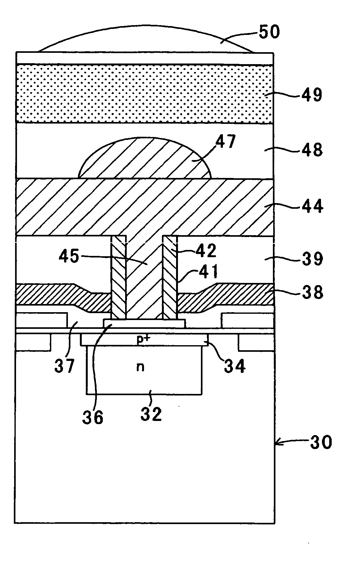
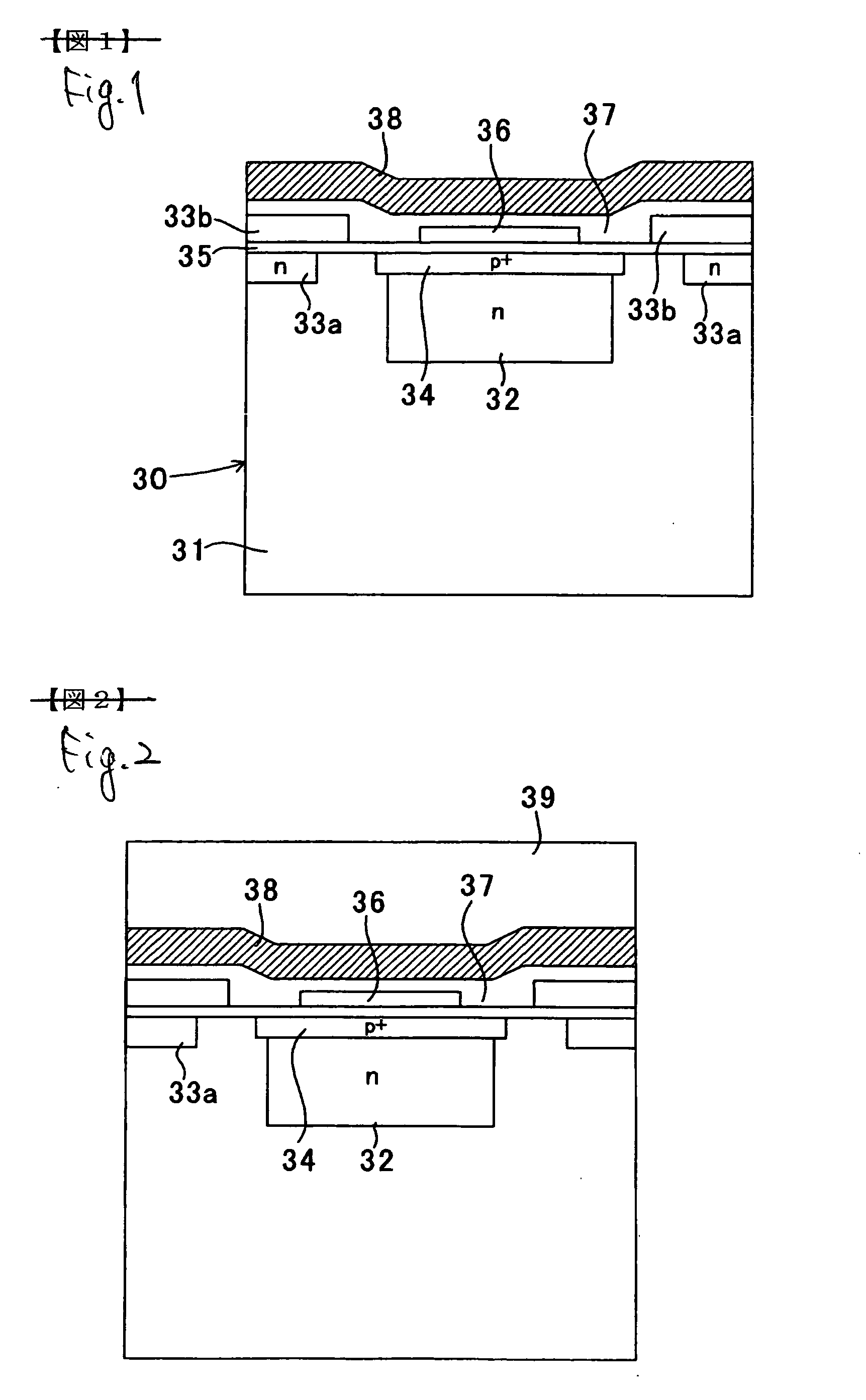
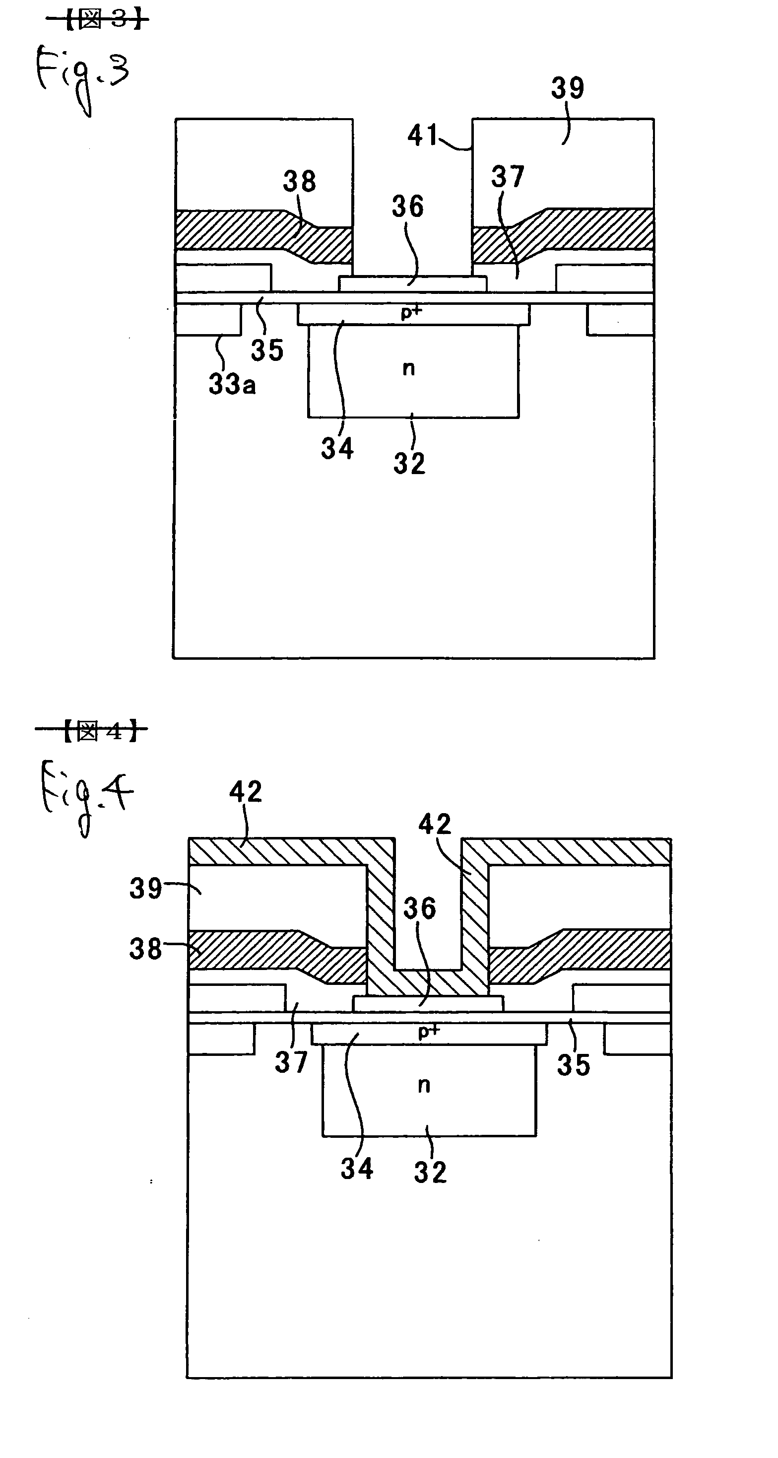
[0032] Hereafter, a description will be given of an embodiment of the invention with reference to the accompanying drawings.

[0033] FIGS. 1 to 8 are diagrams illustrating the procedure of manufacturing a solid-state imaging device in accordance with an embodiment of the invention. In the solid-state imaging device in accordance with this embodiment, as shown in FIG. 1, a p-well layer 31 is formed in a surface portion of an n-type semiconductor substrate 30, and an n region 32 is formed in a surface portion of the p-well layer 31 to thereby form a photodiode. An embedded channel 33a for constituting a vertical transfer path is formed near a side portion of the n region 32, while a p+ diffusion layer 34 for suppressing a dark current is provided on a surface portion of the n region 32. It should be noted that a p-type semiconductor substrate 30 may be provided instead of providing the p-well layer 31.

[0034] The outermost surface of the semiconductor substrate 30 is covered with a gat...


PUM


Abstract

A method of manufacturing a solid-state imaging device, wherein the solid-state imaging device comprising: a semiconductor substrate; a plurality of photodiodes that are formed on a surface of the semiconductor substrate so as to be arranged in an array form; and a light shielding film, provided on or above the surface of the semiconductor substrate, that has a plurality of openings in correspondence with respective ones of the photodiodes, the method comprising: laminating, on the surface of the semiconductor substrate, lamination layers including the light shielding film; opening through holes in the lamination layers, respectively, at positions corresponding to the photodiodes to form the openings in the light shielding film; forming a low refractive index material layer with a predetermined thickness isotropically on a side wall surface of each of the through holes; and filling a remaining hole portion of each of the through holes with a high refractive index material to form an optical waveguide for guiding incident light to each of the photodiodes.

Description

BACKGROUND OF THE INVENTION [0001] 1. Field of the Invention [0002] The present invention relates to a method of manufacturing a solid-state imaging device, and more particularly to a method of manufacturing a solid-state imaging device in which a light-shielding-film opening is provided on a light receiving surface of each photodiode for constituting a pixel. [0003] 2. Description of the Related Art [0004]FIG. 9 is a schematic surface diagram of a CCD-type image sensor which is an example of the solid-state imaging device. In this solid-state imaging device 1, a multiplicity of photodiodes (PDs) 3 are formed on the surface of a semiconductor substrate 2 by being arranged in the form of an array, i.e., in the form of a square lattice in the illustrated example. In addition, a vertical transfer path (VCCD) 4 for receiving and transferring signal charges accumulated by the photodiodes 3 in correspondence with the amounts of light received is provided on a side of each row of the photo...

Claims


Application Information

Patent Timeline
IPC IPC(8): H01L21/00H01L27/14H01L31/10H04N5/335H04N5/369
CPCH01L27/14621H01L27/14625H01L27/14627H01L27/14868H01L27/14632H01L27/14685H01L27/14629
Inventor UYA, SHINJI
Owner FUJIFILM CORP
Why Eureka
Try Eureka