Method and system for error correction in flash memory

a flash memory and error correction technology, applied in the field of integrated circuits, can solve the problems of inability to transfer multiple discrete units of charge to a capacitive cell, inability to transfer multiple discrete units of charge, and inability to accurately detect the error level of the cell, so as to improve the reliability of data read and increase the storage density

Active Publication Date: 2007-07-26
MARVELL ASIA PTE LTD
View PDF21 Cites 298 Cited by
  • Summary
  • Abstract
  • Description
  • Claims
  • Application Information

AI Technical Summary

Benefits of technology

[0022] Many benefits are achieved by way of the present invention over conventional techniques. For example, embodiments of the present invention provide solid state non-volatile memory systems with increased storage density. Moreover, some embodiments improve the reliability of data read from sol...

Problems solved by technology

As with most solid state non-volatile memory devices, flash EEPROMs are susceptible to defects and failures.
Errors result from several factors including the gradual shifting of the threshold level of the memory states as. a result of ambient conditions and stress from normal operations of the memory device including program, erase, and read operations.
During programming, it is more difficult to transfer multiple discrete units of charge to a capacitive cell than it is simply to fully charge or fully discharge the cell.
Thus, uncertainty in the amount of charge transferred to ...

Method used


Image

  • Method and system for error correction in flash memory
  • Method and system for error correction in flash memory
  • Method and system for error correction in flash memory

Examples


Embodiment Construction

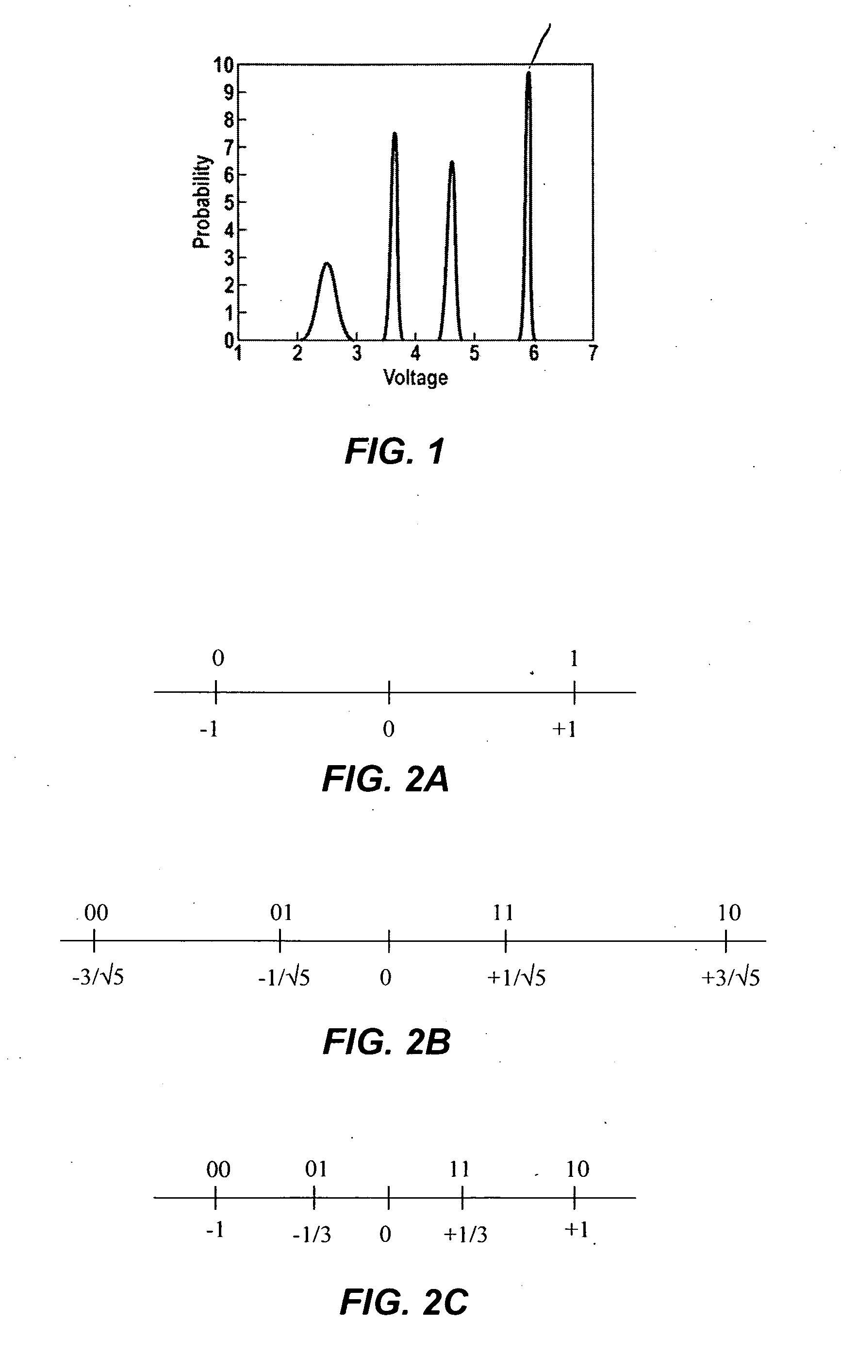
[0042]FIG. 2A is a constellation diagram for an uncoded one bit PAM (pulse amplitude modulation) scheme according to which, information is stored as either a 0 (−1 volts) or a 1 (+1 volts). FIG. 2B is a constellation diagram for a two-bit data modulated using a PAM scheme having an average power of 1. The four states defined by the two bits, namely states (00; 01, 10, and 11) are mapped to one of four possible levels, for example, −3 / √5 volts, −1 / √5 volts, +1 / √5 volts, and +3 / √5 volts. Given these voltages, both the 2-points PAM (2-PAM) and the 4-points PAM (4-PAM) with ½ code rate provide a 1 bit / cell spectral efficiency and are characterized by equal power. For the modulation scheme illustrated by FIG. 2B, the 4-state code with Gray mapping reduces bit error rate over the 4-state natural mapping.

[0043] In solid state non-volatile memory devices, the maximum voltage applied at the floating gate limits the maximum voltage available for mapping of multi-level symbols. This...


PUM


Abstract

A solid state non-volatile memory unit. The memory unit includes a multi-level solid state non-volatile memory array adapted to store data characterized by a first number of digital levels. The memory unit also includes an analog-to-digital converter having an input and an output. The input of the analog-to-digital converter is adapted to receive data from the multi-level solid state non-volatile memory array. The output of the analog-to-digital converter is adapted to output a digital signal characterized by a second number of digital levels greater than the first number of digital levels.

Description

CROSS-REFERENCES TO RELATED APPLICATIONS [0001] The present application claims benefit under 35 U.S.C. § 119(e) of the following U.S. provisional applications, all of which are commonly assigned and incorporated herein by reference in their entirety: [0002] Provisional Application No. 60 / 760,622, entitled “Flash Memory—Error Correction Issues,” filed on Jan. 20, 2006; [0003] Provisional Application No. 60 / 761,888, entitled “Increase Storage Capacity of Flash Memory through Coding and Signal Processing,” filed on Jan. 25, 2006; and [0004] Provisional Application No. 60 / 771,621, entitled “Increase Storage Capacity of Flash Memory through Coding and Signal Processing,” filed on Feb. 8, 2006; [0005] The present application is also related to concurrently filed U.S. patent application Ser. No. ______ (Attorney Docket No. MP0916), entitled “Flash Memory with Coding and Signal Processing,” commonly assigned and incorporated herein by reference in its entirety.BACKGROUND OF THE INVENTION [0...

Claims


Application Information

Patent Timeline
IPC IPC(8): G11C16/04
CPCG06F11/1072G11C7/02G11C7/1006G11C7/16G11C11/56G11C11/5621G11C16/10G11C27/005G11C29/00G11C2029/0411G11C2207/16G06F11/1666G11C2211/562G11C2211/563G06F11/1068G11C29/42G11C16/04G06F2212/403H03M13/1177H03M13/1515
Inventor RAMAMOORTHY, ADITYAWU, ZININGSUTARDJA, PANTAS
Owner MARVELL ASIA PTE LTD
Why Eureka
Try Eureka