Manufacturing method of semiconductor device

a manufacturing method and semiconductor technology, applied in the field of manufacturing methods of semiconductor devices, can solve the problems of small damage given to a wafer, large consumption of blades, low durability, etc., and achieve the effects of preventing blinding of blades, preventing deterioration of cutting surface quality, and suppressing the reduction of cutting capacity

Active Publication Date: 2007-07-26
RENESAS ELECTRONICS CORP
View PDF4 Cites 18 Cited by
  • Summary
  • Abstract
  • Description
  • Claims
  • Application Information

AI Technical Summary

Benefits of technology

[0013]According to the present invention, when cutting the wafer on which the low dielectric constant film was formed, blinding of a blade

Problems solved by technology

Since the blade surface of a resin bonding blade is soft, its damage given to a wafer is small.
However, the above-mentioned blade has the large consumption at the time of cutting, and its durability is low.
For this reason, jig replacement frequency increases and a manufacturing cost rises.
When the wafer surface was cut using the above-mentioned

Method used


Image

  • Manufacturing method of semiconductor device
  • Manufacturing method of semiconductor device
  • Manufacturing method of semiconductor device

Examples


embodiment 1

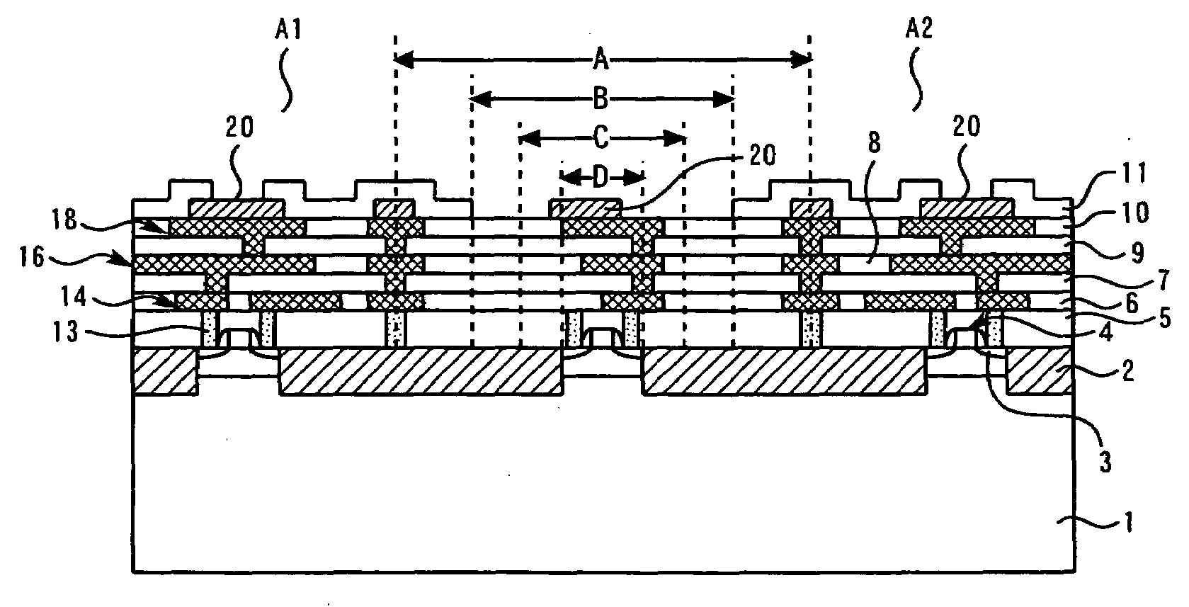
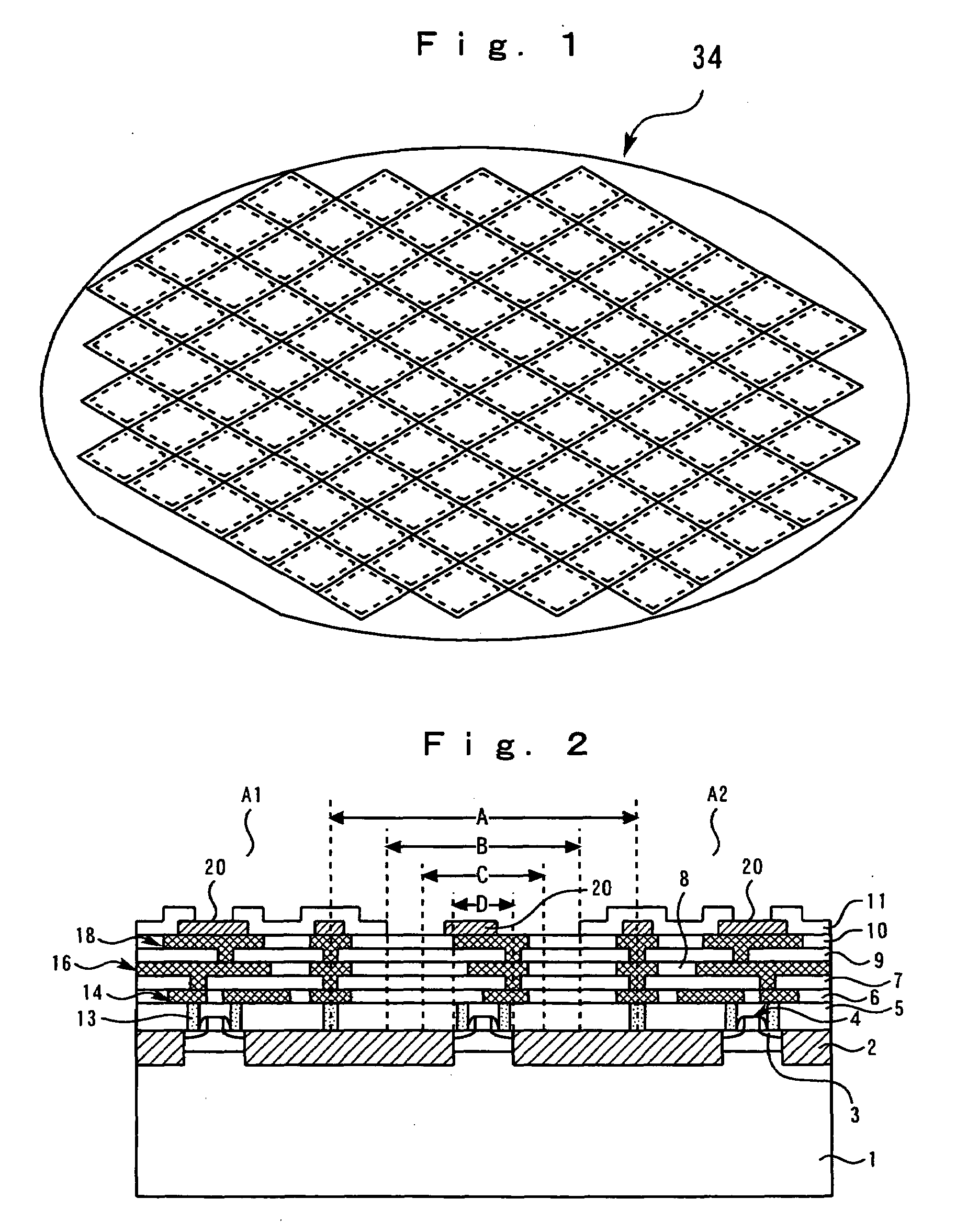
[0047]The manufacturing method of the semiconductor device of the present invention is explained. Here, the example which cuts the wafer in which elements, such as a transistor, the wiring, and the insulating film were formed on the silicon substrate, in the shape of a semiconductor chip by dicing is explained.

[0048]The perspective view of the wafer after forming elements, such as a transistor, a wiring, and an insulating film on a silicon substrate is shown in FIG. 1, and a cross-sectional view is shown in FIG. 2. Back surface polish of the thickness of a wafer is done to the thickness of about 250 μm by the back-grinding step on the back surface of a wafer which is not illustrated. As the method of back surface polish, a mechanical means, a chemical means, the case where a mechanical means and a chemical means are used together, etc. can choose suitably. Device regions A1 and A2 are formed on silicon substrate 1, and these regions adjoin. Between these regions, dicing line A which...

embodiment 2

[0091]This embodiment explains the step until it performs the assembly of a semiconductor chip and results in shipment after performing the dicing step shown by Embodiment 1.

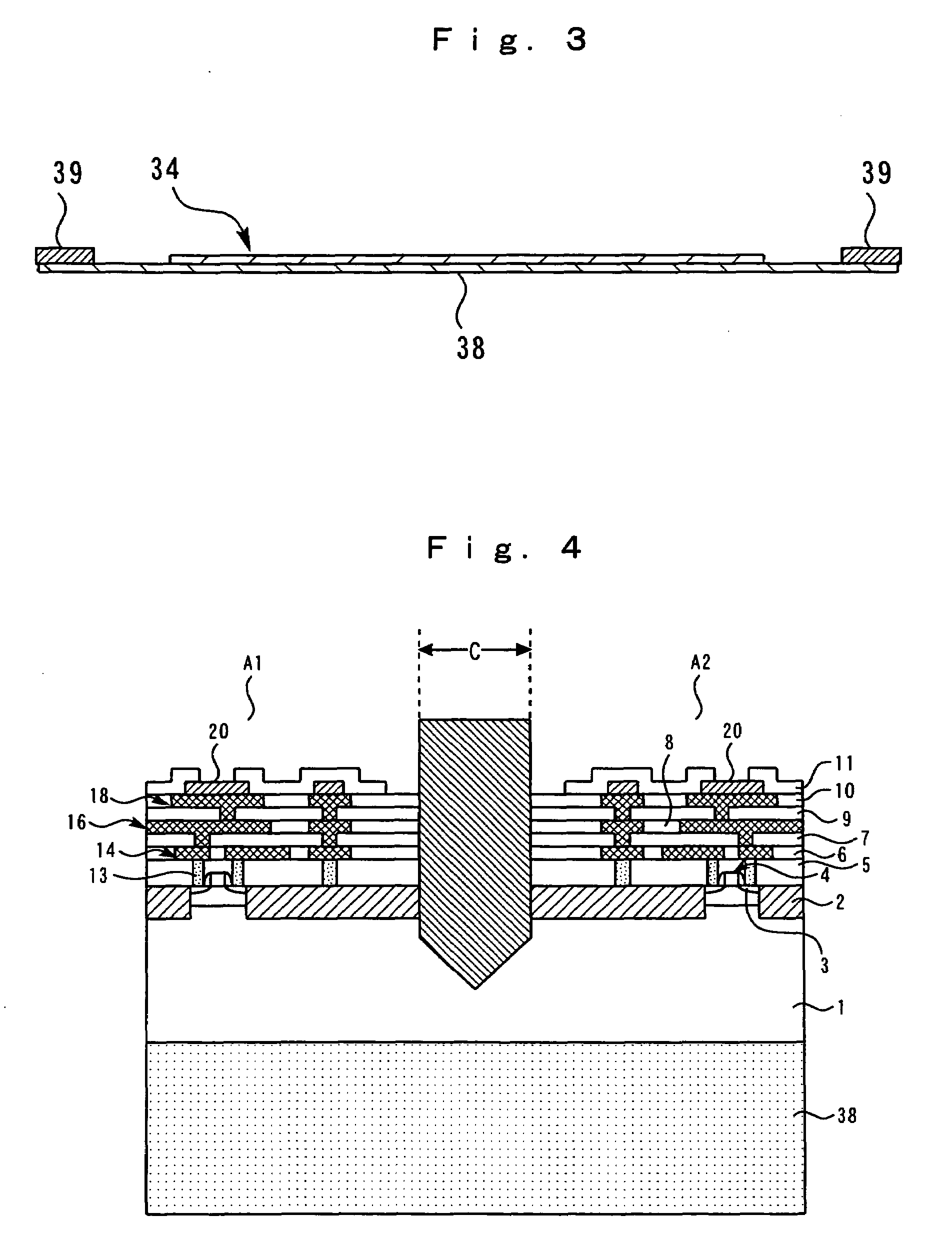
[0092]The process flow comprising the dicing step shown by Embodiment 1, and steps until it ships after that is shown in FIG. 25. First, wafer 34 in which elements, such as a transistor, were formed on the silicon substrate is prepared as described in FIG. 1 (S1). Next, like the description to FIG. 3, dicing tape 38 is stuck on the back surface of wafer 34, and it mounts (S2). Next, dicing is performed by the method shown by Embodiment 1 (S3). Next, ultraviolet rays are irradiated in order to reduce the adhesive power of dicing tape 38 (S4). Hereby, peeling of dicing tape 38 in a later step can be made easy. Next, like the description to FIG. 26, dicing tape 38 is peeled and semiconductor chip 41 cut per chip is picked up (S5).

[0093]In order to assemble semiconductor chip 41 picked up by above S5, like a descrip...


PUM


Abstract

Size of a chipping is made small, suppressing blinding of a blade, when performing dicing of a wafer.
When cutting a wafer, cutting is performed so that the portion of a V character-shaped shoulder may enter below the front surface of a wafer (depth Z2 from a substrate front surface) using the metal-bond blade which includes the abrasive particle whose fineness number is more than #3000, and whose point is V character form. By processing it in this way, cutting resistance goes up and blinding of a blade can be prevented. Hereby, the size of a chipping can be suppressed small, preventing blinding of a blade.

Description

CROSS-REFERENCE TO RELATED APPLICATION [0001]The present application claims priority from Japanese patent application No. 2006-12367 filed on Jan. 20, 2006, the content of which is hereby incorporated by reference into this application.[0002]1. Field of the Invention[0003]The present invention relates to a manufacturing method of a semiconductor device, and particularly relates to a manufacturing method of a semiconductor device having a step which cuts the wafer in which low dielectric constant films, such as an SiOC film, were formed on the substrate, by a dicing blade.[0004]2. Description of the Background Art[0005]In the manufacturing method of a semiconductor device, after the manufacturing process on a wafer is completed, it is cut by the dicing blade etc. per semiconductor chip. In recent years, low dielectric constant films, such as SiOC, are formed on the wafer for the capacity reduction between wirings.[0006]Since a low dielectric constant film is a vulnerable film, when c...

Claims


Application Information

Patent Timeline
IPC IPC(8): H01L21/00
CPCH01L21/78B28D5/022H01L24/97H01L2224/32225H01L2224/48227H01L2224/73265H01L2224/83192H01L2924/15311H01L2924/181H01L2924/00012H01L2924/00H01L21/82
Inventor IZUMI, NAOKI
Owner RENESAS ELECTRONICS CORP
Why Eureka
Try Eureka