

Imaging device
a technology of imaging device and image sensor, which is applied in the field of imaging device, can solve the problems of disadvantageous and difficult miniaturization of imaging device (cmos image sensor), similar to the case of aforementioned conventional ccd image sensor
- Summary
- Abstract
- Description
- Claims
- Application Information
AI Technical Summary
Problems solved by technology
Method used
Image

Examples
first embodiment
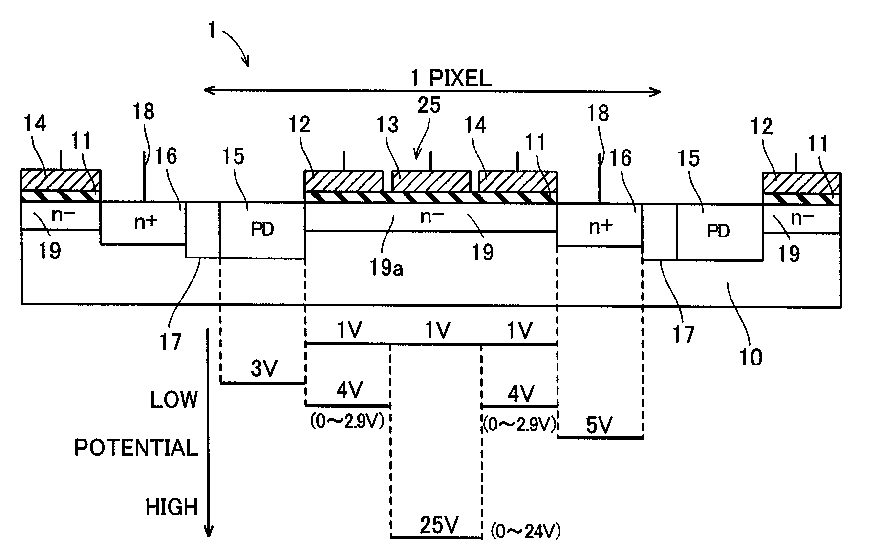
[0029]A structure of a CMOS image sensor according to a first embodiment will be now described with reference to FIGS. 1 to 4.
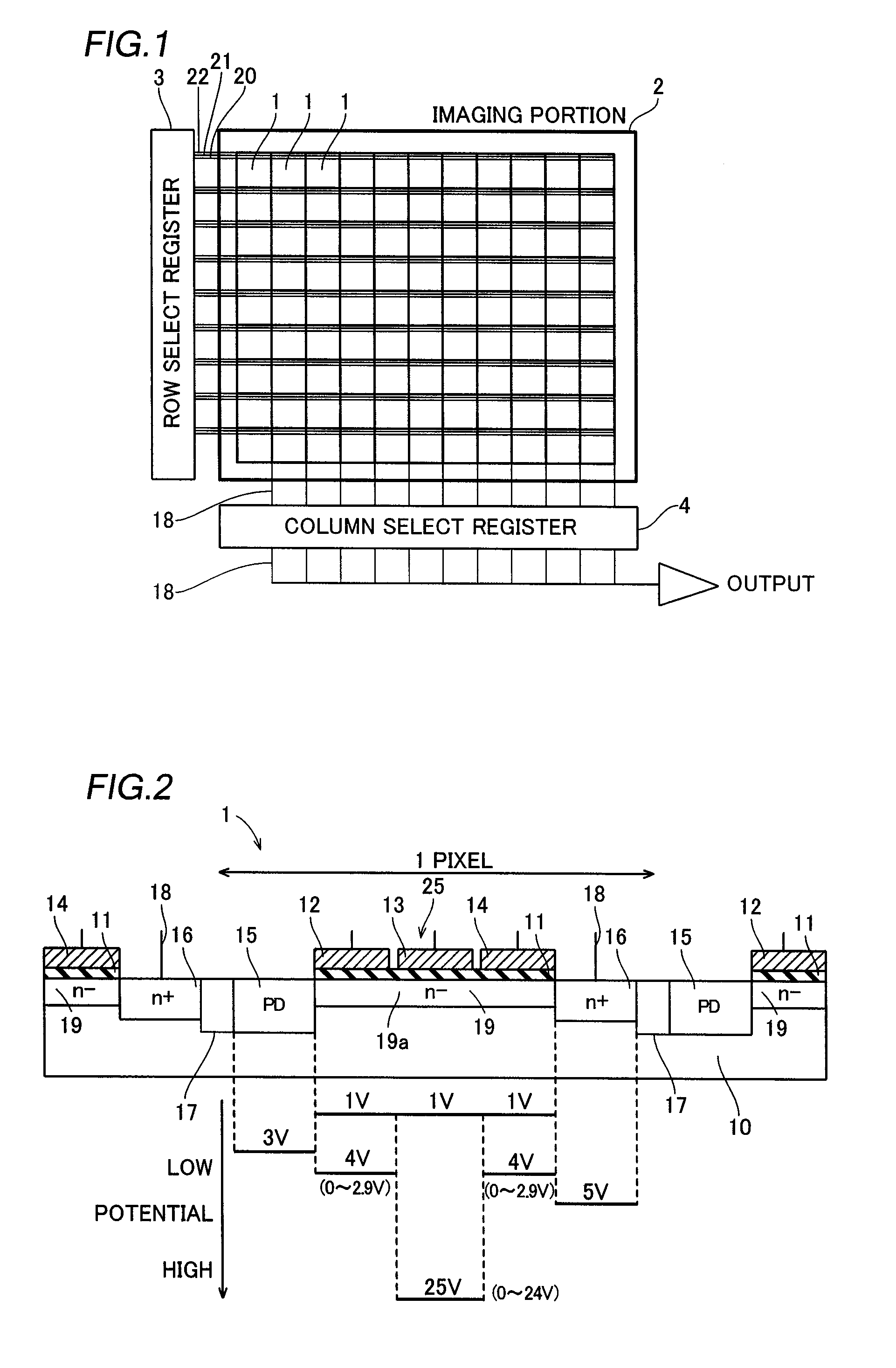
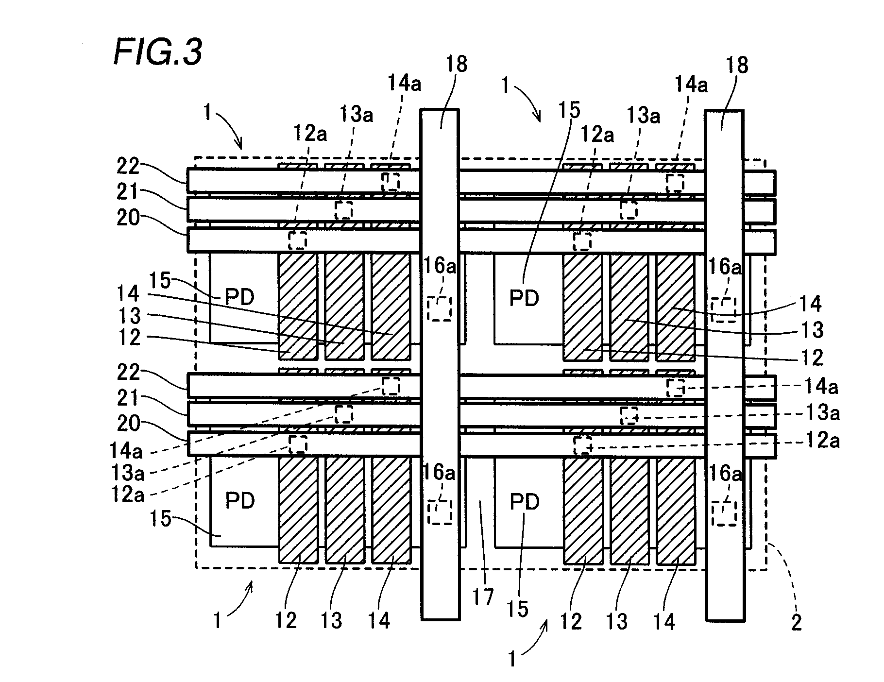
[0030]The CMOS image sensor according to the first embodiment comprises an imaging portion 2 including a plurality of pixels 1, a row select register 3 and a column select register 4 as shown in FIG. 1. Each pixel 1 is constituted by a p-type silicon substrate 10, a gate insulating film 11, three gate electrodes of one transfer gate electrode 12, one multiplication gate electrode 13 and one readout gate electrode 14, a photodiode portion (PD) 15, a floating diffusion region 16 consisting of an n-type impurity region and an element separation region 17, as shown in FIG. 2. The gate insulating films 11 are formed on a surface of the p-type silicon substrate 10 at prescribed intervals. The transfer gate electrode 12, the multiplication gate electrode 13 and the readout gate electrode 14 are formed in prescribed regions of an upper surface of each gate insulating...
second embodiment
[0051]With reference to FIG. 9, in a second embodiment, a structure of a CMOS image sensor including pixels 30 so formed that photodiode portions 15 are adjacent to readout gate electrodes 14 respectively will be described dissimilarly to the aforementioned first embodiment.
[0052]As shown in FIG. 9, in a cross-sectional structure of the pixels 30 of the CMOS image sensor according to the second embodiment, element separation regions 17 are formed on a surface of a p-type silicon substrate 10 for separating the pixels 30. The photodiode portion 15 is so formed on the surface of the p-type silicon substrate 10 of each pixel 30 surrounded by the element separation regions 17 as to hold a transfer channel 31 consisting of an n-type impurity region spaced at a prescribed interval from the one of the element separation regions 17. A floating diffusion region 16 is so formed on the surface of the p-type silicon substrate 10 of each pixel 30 as to hold a transfer channel 32 consisting of an...
third embodiment
[0064]With reference to FIG. 11, in a third embodiment, a structure of a CMOS image sensor including pixels 40 so formed that transfer gate electrodes 42 are formed on photodiode portions 15 respectively will be described dissimilarly to the aforementioned first embodiment.
[0065]As shown in FIG. 11, in a cross-sectional structure of the pixels 40 of the CMOS image sensor according to the third embodiment, gate insulating films 41 are formed on upper surfaces corresponding to the photodiode portions 15 and transfer channels 19 of a p-type silicon substrate 10. Each transfer gate electrode 42 is formed in a region corresponding to the photodiode portion 15 on the upper surface of the gate insulating film 41. The transfer gate electrodes 42 are examples of the “second transfer electrode” in the present invention. A transfer gate electrode 12, a multiplication gate electrode 13 and a readout gate electrode 14 are formed in regions corresponding to each transfer channel 19 on the upper s...
PUM
 Abstract
Description
Claims
Application Information