Delay-locked loop circuit of a semiconductor device and method of controlling the same

a technology of delay-locked loop circuit and semiconductor device, which is applied in the direction of pulse automatic control, pulse manipulation, pulse technique, etc., can solve the problems of delay time applied to the external clock signal and may be changed, and the synchronization between the external clock signal and the internal clock signal may not be completed

Inactive Publication Date: 2007-08-02
SAMSUNG ELECTRONICS CO LTD
View PDF8 Cites 19 Cited by
  • Summary
  • Abstract
  • Description
  • Claims
  • Application Information

AI Technical Summary

Problems solved by technology

When the voltage supplied to the DLL is changed, the delay time applied to the external clock signal may be changed and the synchronization between the external clock signal and the internal clock signal may not be completed.

Method used


Image

  • Delay-locked loop circuit of a semiconductor device and method of controlling the same
  • Delay-locked loop circuit of a semiconductor device and method of controlling the same
  • Delay-locked loop circuit of a semiconductor device and method of controlling the same

Examples


Embodiment Construction

[0019]Exemplary embodiments of the present invention will be described in detail with reference to the accompanying drawings. Like reference numerals refer to similar or identical elements throughout the description of the figures.

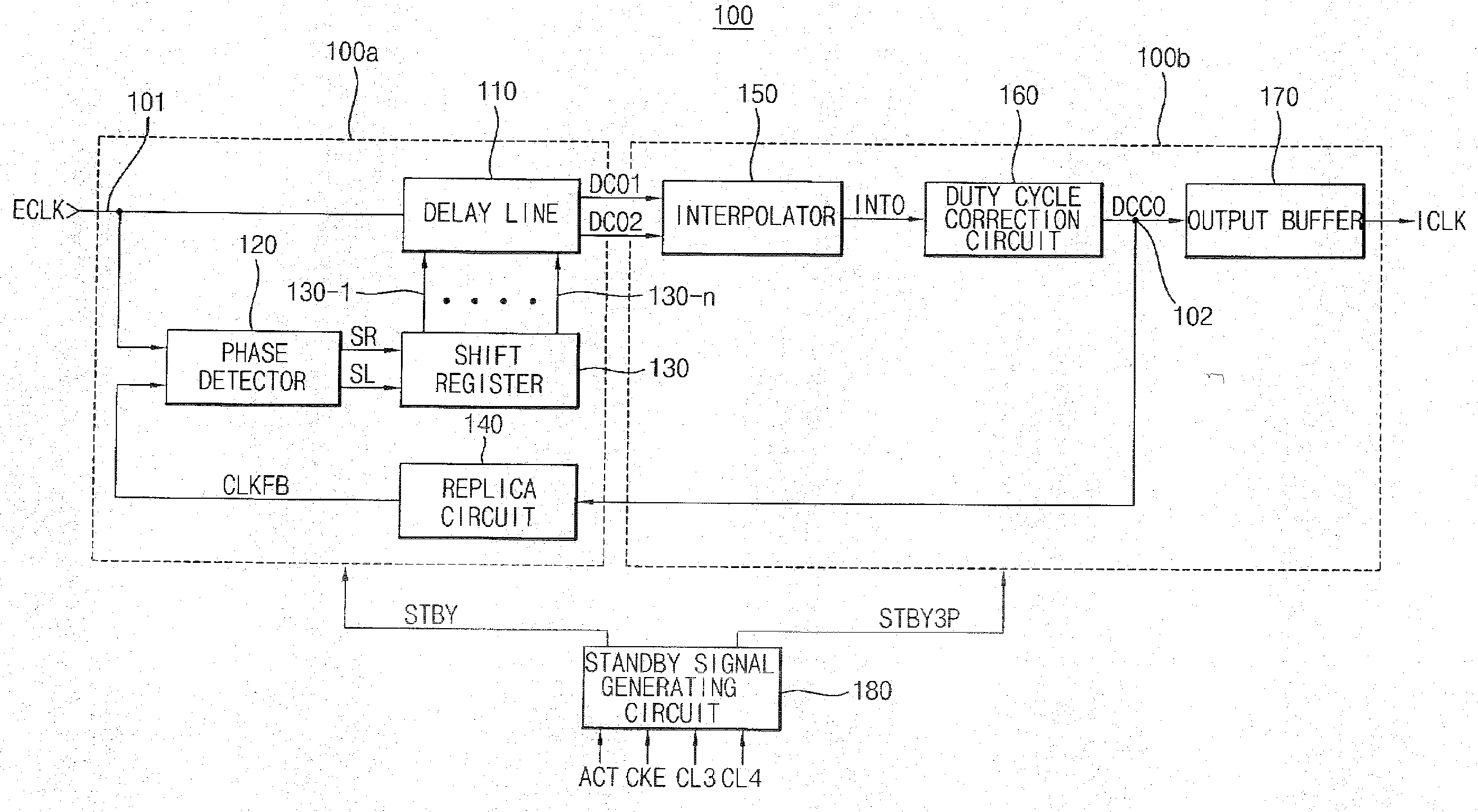
[0020]FIG. 1 is a block diagram illustrating a delay-locked loop (DLL) circuit according to an exemplary embodiment of the present invention.

[0021]Referring to FIG. 1, the DULL circuit 100 includes a standby signal generating circuit 180, a front stage circuit 100a, and a back stage circuit 100b.

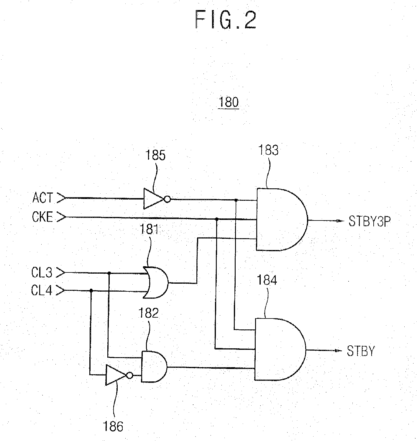
[0022]The standby signal generating circuit 180 generates a first standby signal STBY and a second standby signal STBY3P. For example, the standby signal generating circuit 180 may generate the first standby signal STBY and the second standby signal STBY3P in response to an active signal ACT a clock enable signal CKE, a first column address strobe (CAS) latency signal CL3, and a second CAS latency signal CL4.

[0023]The front stage circuit 100a compares the phase of...


PUM


Abstract

A delay-locked loop (DLL) circuit includes a standby signal generating circuit, a front stage circuit, and a back stage circuit. The standby signal generating circuit generates a first standby signal and a second standby signal in response to an active signal, a crock enable signal, a first column address strobe (CAS) latency signal, and a second CAS latency signal. The front stage circuit compares the phase of an external clock signal and the phase of a feedback signal and delays the external clock signal based on the phase difference between the external clock signal and the feedback signal to generate a first clock signal. The back stage circuit executes interpolation and duty-cycle correction on the first clock signal.

Description

CROSS-REFERENCE TO RELATED PATENT APPLICATION[0001]This application claims priority under 35 USC § 119 to Korean Patent Application No. 2006-9703, filed on Feb. 1, 2006, the disclosure of which is herein incorporated by reference in its entirety.BACKGROUND OF THE INVENTION[0002]1. Technical Field[0003]The present disclosure relates to a delay-locked loop circuit and, more particularly, to a delay-locked loop circuit of a semiconductor device and a method of controlling the same.[0004]2. Discussion of Related Art[0005]A delay-locked loop (DLL) circuit is frequently used in semiconductor integrated circuits to generate an internal clock signal. In a conventional DLL the internal crock signal is generated by delaying a system crock signal or an external clock signal by a predetermined time. The DLL detects the phase difference between the internal crock signal and the external clock signal and controls a delay time by performing a shift operation to synchronize the internal clock signa...

Claims


Application Information

Patent Timeline
Patent Type & Authority Applications(United States)
IPC IPC(8): H03L7/06
CPCH03K5/13H03L7/0814H03K2005/00052H03L7/0816A47K7/04
Inventor BYUN, YOUNG-YONGLEE, DONG-JINLEE, HI-CHOON
Owner SAMSUNG ELECTRONICS CO LTD
Why Eureka
Try Eureka