Selective CESL structure for CMOS application

a technology of cmos and cmos, applied in the field of mos devices, metal oxidesemiconductor devices, structure and manufacturing methods of mos devices, can solve the problems of reducing the reliability of pmos devices formed using conventional methods, reducing the nbti, and constant effort in scaling of vlsi circuits

Inactive Publication Date: 2007-08-09
TAIWAN SEMICON MFG CO LTD
View PDF31 Cites 21 Cited by
  • Summary
  • Abstract
  • Description
  • Claims
  • Application Information

AI Technical Summary

Benefits of technology

[0014] Since the barrier layer prevents hydrogen from traveling through and forming bonds with s

Problems solved by technology

The scaling of VLSI circuits is a constant effort.
When device dimensions are reduced to 130 nm and lower, particular 65 nm and lower, conventional methods for improving device drive current, such as shortening gate length and increasing gate capacitance, become difficult to implement.
PMOS devices formed using the conventional methods suffer reliability issues, however.
These bonds may be broken later

Method used


Image

  • Selective CESL structure for CMOS application
  • Selective CESL structure for CMOS application
  • Selective CESL structure for CMOS application

Examples


Embodiment Construction

[0019] The making and using of the presently preferred embodiments are discussed in detail below. It should be appreciated, however, that the present invention provides many applicable inventive concepts that can be embodied in a wide variety of specific contexts. The specific embodiments discussed are merely illustrative of specific ways to make and use the invention, and do not limit the scope of the invention.

[0020] The intermediate stages of manufacturing a preferred embodiment of the present invention are illustrated in FIGS. 2 through 8. Variations of the preferred embodiments are then discussed. Throughout the various views and illustrative embodiments of the present invention, like reference numbers are used to designate like elements.

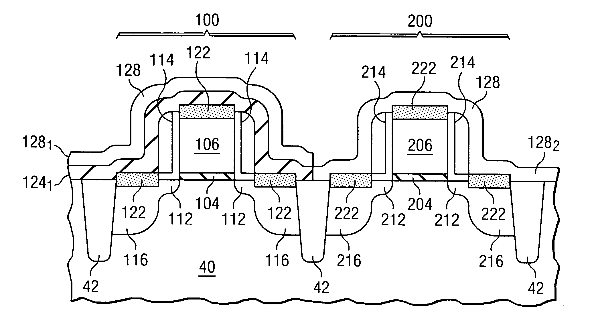
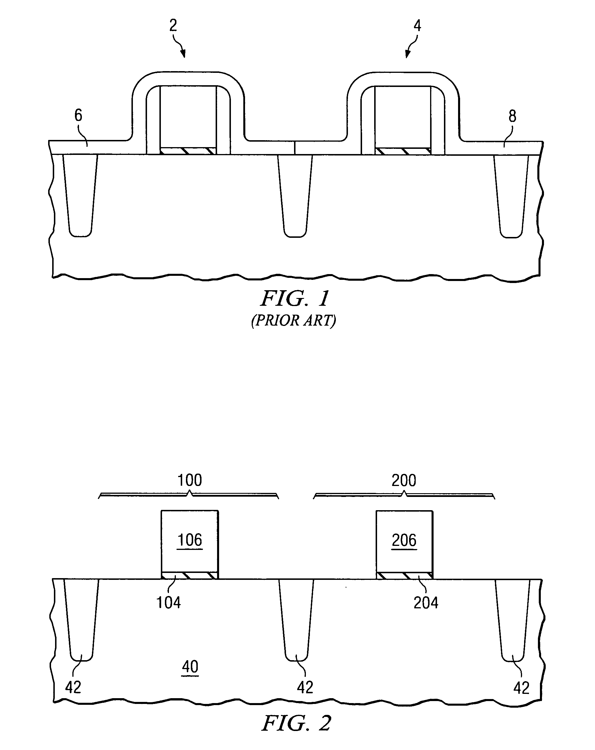
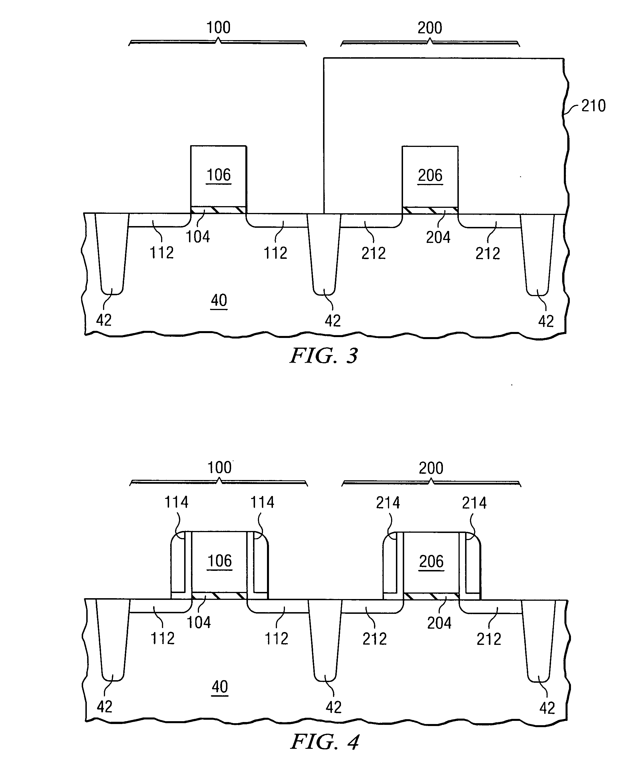
[0021]FIG. 2 illustrates gate stacks formed over a substrate 40 comprising two regions, a region 100 for forming a PMOS device and a region 200 for forming an NMOS device, which are isolated by shallow trench isolations (STI) 42 formed in the...


PUM


Abstract

A PMOS device less affected by negative bias time instability (NBTI) and a method for forming the same are provided. The PMOS device includes a barrier layer over at least a portion of a gate structure, a gate spacer, and source/drain regions of a PMOS device. A stressed layer is then formed over the barrier layer. The barrier layer is preferably an oxide layer and is preferably not formed for NMOS devices.

Description

TECHNICAL FIELD [0001] This invention relates generally to semiconductor devices, and more particularly to metal-oxide-semiconductor (MOS) devices, and even more particularly to the structure and manufacturing method of MOS devices having stressed channel regions. BACKGROUND [0002] The scaling of VLSI circuits is a constant effort. With circuits becoming smaller and faster, improvement in device drive current is becoming more important. When device dimensions are reduced to 130 nm and lower, particular 65 nm and lower, conventional methods for improving device drive current, such as shortening gate length and increasing gate capacitance, become difficult to implement. Further methods such as increasing carrier mobility have thus been explored. [0003] Among efforts made to enhance carrier mobility, forming a stressed silicon channel is a known practice. Stress, sometimes referred to as strain, can enhance electron and hole mobility. The performance of a metal-oxide-semiconductor (MOS...

Claims


Application Information

Patent Timeline
IPC IPC(8): H01L29/76H01L21/8238
CPCH01L21/823807H01L21/823814H01L21/823864H01L29/7848H01L29/66636H01L29/7843H01L29/665
Inventor CHEN, CHIA-LINCHEN, MIN-JANWANG, JAU-JEY
Owner TAIWAN SEMICON MFG CO LTD
Why Eureka
Try Eureka