Method for manufacturing a mos transistor

a metaloxide semiconductor and transistor technology, applied in transistors, basic electric elements, electric devices, etc., can solve the problems of reducing access resistance, reducing the sce and nbti, and limiting the process tolerance of semiconductor devices. , to achieve the effect of reducing sce and nbti, reducing both sce and nbti, and superior process compatibility

Inactive Publication Date: 2009-05-07
UNITED MICROELECTRONICS CORP
View PDF12 Cites 0 Cited by
  • Summary
  • Abstract
  • Description
  • Claims
  • Application Information

AI Technical Summary

Benefits of technology

[0015]According to the method for manufacturing a MOS transistor provided by the present invention, a thermal treatment is performed to repair the damaged lattice in the surface of the semiconductor substrate before forming the source/drain extension regions, therefore NBTI is reduced. Since the thermal treatm

Problems solved by technology

However, scales of the semiconductor devices are limited by process tolerance, electric characteristics directly related to the device itself, and requirement of high reliability to the integrated circuits.
With the device scaling down, it's getting difficult to control the junction depth (Xj) of the source/drain extension regions 20 and to reduce the access resistance.
Although such solution is able to reduce SCE, it generates another adverse influence on reliability of the MOS transistor.
It is noticeable that such process damages lattice in surface of the substrate 10.
It also adversely affects interface between the nitrogen-contained gate oxide layer 12 and the substrate 10.
Since heat budget is limited for reducing SCE, the limited heat is not sufficient to repair the damaged lattice in the surface of the substrate 10.
Therefore a negative shift of threshold voltage, namely negative bias temperature inst

Method used


Image

  • Method for manufacturing a mos transistor
  • Method for manufacturing a mos transistor
  • Method for manufacturing a mos transistor

Examples


Embodiment Construction

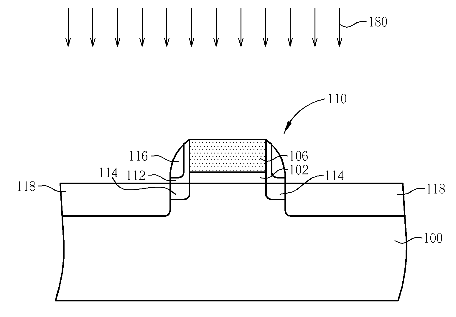
[0021]Please refer to FIGS. 4-8, which are schematic drawings illustrating a method for manufacturing a MOS transistor according to a first preferred embodiment of the present invention. As shown in FIG. 4, a semiconductor substrate 100 having a gate dielectric layer and a polysilicon layer 104 formed thereon is provided. For decreasing current leakage, offering a better barrier to boron, and improving performance of the transistor, nitrogen is implanted into the gate dielectric layer by a high temperature plasma nitridation process such as DPN, thus a nitrogen-contained gate dielectric layer 102 is obtained. It is noteworthy that the lattice in the surface of the semiconductor substrate 100 is often damaged, interface between the semiconductor substrate 100 and the nitrogen-contained gate dielectric layer 102 is adversely affected in such process, and consequently reliability of the transistor is adversely affected due to NBTI. Therefore, a thermal treatment 150 is performed to rep...


PUM


Abstract

A method for manufacturing a MOS transistor includes performing a thermal treatment to repair damaged substrate before forming source/drain extension regions, accordingly negative bias temperature instability (NBTI) is reduced. Since the thermal treatment is performed before forming the source/drain extension regions, heat budget for forming the source/drain extension regions and junction depth and junction profile of the source/drain extension would not be affected. Therefore the provided method for manufacturing a MOS transistor is capable of reducing short channel effect and possesses a superior process compatibility.

Description

BACKGROUND OF THE INVENTION [0001]1. Field of the Invention[0002]The invention relates to a method for manufacturing a metal-oxide semiconductor (MOS) transistor, and more particularly, to a method capable of reducing negative bias temperature instability (NBTI) of a MOS transistor.[0003]2. Description of the Prior Art[0004]In accordance with a demand and tendency toward higher density and higher integration to integrated circuit and semiconductor devices, dimensions of semiconductor devices are continually shrunk. However, scales of the semiconductor devices are limited by process tolerance, electric characteristics directly related to the device itself, and requirement of high reliability to the integrated circuits.[0005]Please refer to FIGS. 1-3, which are drawings illustrating a conventional method for manufacturing a MOS transistor. As shown in FIG. 1, a substrate 10 is firstly provided. The substrate 10 includes a polysilicon layer and a gate oxide layer formed thereon. For sa...

Claims


Application Information

Patent Timeline
IPC IPC(8): H01L21/336
CPCH01L21/28035H01L29/6659H01L21/28247H01L21/28202
Inventor WU, MENG-YILEE, KUN-HSIENHUANG, CHENG-TUNGHUNG, WEN-HANTING, SHYH-FANNJENG, LI-SHIANSHIH, CHUNG-MINCHENG, YAO-CHINCHENG, TZYY-MING
Owner UNITED MICROELECTRONICS CORP
Why Eureka
Try Eureka