Two-dimensional material/semiconductor hetero-junction tunneling transistor and preparation method thereof

A two-dimensional material and semiconductor technology, applied in the field of nanoelectronics, can solve problems such as difficult to achieve high doping, achieve low power consumption, large on-state current, and increase the effect of on-state current

Active Publication Date: 2017-08-29
PEKING UNIV
View PDF6 Cites 14 Cited by
  • Summary
  • Abstract
  • Description
  • Claims
  • Application Information

AI Technical Summary

Problems solved by technology

However, it is difficult to achieve high doping in two-dimensional materials to form a P-I-N structure in experiments. The physical and chemical doping currently studied has problems such as stability, and it still faces great challenges in experimental preparation.

Method used


Image

  • Two-dimensional material/semiconductor hetero-junction tunneling transistor and preparation method thereof
  • Two-dimensional material/semiconductor hetero-junction tunneling transistor and preparation method thereof
  • Two-dimensional material/semiconductor hetero-junction tunneling transistor and preparation method thereof

Examples


Embodiment Construction

[0054] The present invention will be further described below by example. It should be noted that the purpose of the disclosed embodiments is to help further understand the present invention, but those skilled in the art can understand that various replacements and modifications are possible without departing from the spirit and scope of the present invention and the appended claims of. Therefore, the present invention should not be limited to the content disclosed in the embodiments, and the protection scope of the present invention is subject to the scope defined in the claims.

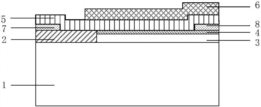
[0055] A specific example of the preparation method of the present invention includes Figure 3 to Figure 10 Process steps shown:

[0056] 1) Using a bulk silicon wafer with a crystal orientation of (100) as the semiconductor substrate (1), using ion implantation BF 2 + P-type doping is carried out on the semiconductor substrate by the method, the doping energy is 40KeV, and the region other than...


PUM


Abstract

The invention discloses a tunneling field effect transistor based on a two-dimensional material/semiconductor hetero-junction and a preparation method thereof. A device forms an interleaved energy band structure in the off state through the energy band design, namely, a tunneling window is inexistent between the two-dimensional material and the semiconductor material, and the ultra-low off-state current can be acquired; the grid voltage can be applied to regulate an energy band alignment way at the two-dimensional material/semiconductor hetero-junction so that the device can form the staggered energy band structure in the on-state, and the effective tunneling barrier height is a negative value; and meanwhile, the current carrier tunnels to a channel region from a source region to realize the direct tunneling, thereby acquiring large on-state current. The device adopts the highly-doped three-dimensional semiconductor material as the source region material, and the three-dimensional semiconductor material and the metal source electrode are unipotential; since the thickness of the two-dimensional material is ultra-thin, the grid voltage can regulate the two-dimensional material and the energy band at the two-dimensional material/semiconductor hetero-junction interface, thereby acquiring an ideal grid control capacity. The tunneling field effect transistor disclosed by the invention is simple in process, and large in compatibility with the traditional semiconductor process.

Description

technical field [0001] The invention belongs to the technical field of nanoelectronics, and in particular relates to a tunneling field effect transistor based on a two-dimensional material / semiconductor heterojunction and a preparation method thereof. Background technique [0002] With the reduction of traditional MOSFET feature size and the improvement of integration, the operating voltage and threshold voltage of the device are gradually reduced. The ensuing short-channel effect is more obvious, and the drain-induced barrier reduction and source-drain band-band tunneling will increase the leakage current and power consumption of the device. In addition, due to the current mechanism of MOSFET thermal emission, its subthreshold slope is limited by the thermal potential, and there is a theoretical limit of 60mV / dec, which cannot be reduced with the reduction of device size, which leads to a further increase in the leakage current of the device and power consumption. The prob...

Claims


Application Information

Patent Timeline
Patent Type & Authority Applications(China)
IPC IPC(8): H01L29/739H01L21/331
Inventor 黄如贾润东黄芊芊赵阳王慧敏陈诚
Owner PEKING UNIV
Why Eureka
Try Eureka