
Light-emitting diode and manufacturing method thereof

A technology of light-emitting diodes and manufacturing methods, which is applied in the direction of electrical components, circuits, semiconductor devices, etc., and can solve the problems that the uniform diffusion of current does not have obvious effects, reduces other properties of materials, and the uniform diffusion of current does not achieve ideal effects, etc. , to increase ESD performance and prevent current congestion

Inactive Publication Date: 2011-09-14
ENRAYTEK OPTOELECTRONICS
View PDF7 Cites 6 Cited by
  • Summary
  • Abstract
  • Description
  • Claims
  • Application Information

AI Technical Summary

Problems solved by technology

[0004] CN101694858A patent proposes an LED epitaxial structure and its manufacturing method, the structure is inserted between the light-emitting layer and the p-type nitride layer by undoped Al x In y Ga 1-x-y n-layer and p-type Al x In y Ga 1-x-y The insertion layer composed of n layers alternately protects the ESD protection performance of the material, and does not reduce other properties of the material, but it does not have a significant effect on the uniform diffusion of current.
[0005] CN101183642A patent proposes a preparation method of p-GaN low-resistance ohmic contact, which uses the p-InGaN / p-AlGaN superlattice layer as the top layer of p-GaN to reduce the contact resistance, but this method is not good for the uniformity of the current Diffusion did not have the desired effect

Method used


Image

  • Light-emitting diode and manufacturing method thereof
  • Light-emitting diode and manufacturing method thereof
  • Light-emitting diode and manufacturing method thereof

Examples


Embodiment Construction

[0029] The light-emitting diode and its manufacturing method proposed by the present invention will be further described in detail below with reference to the drawings and specific embodiments. According to the following description and claims, the advantages and features of the present invention will be clearer. It should be noted that the drawings all adopt very simplified forms and all use imprecise ratios, which are only used for the purpose of conveniently and clearly assisting in describing the embodiments of the present invention.

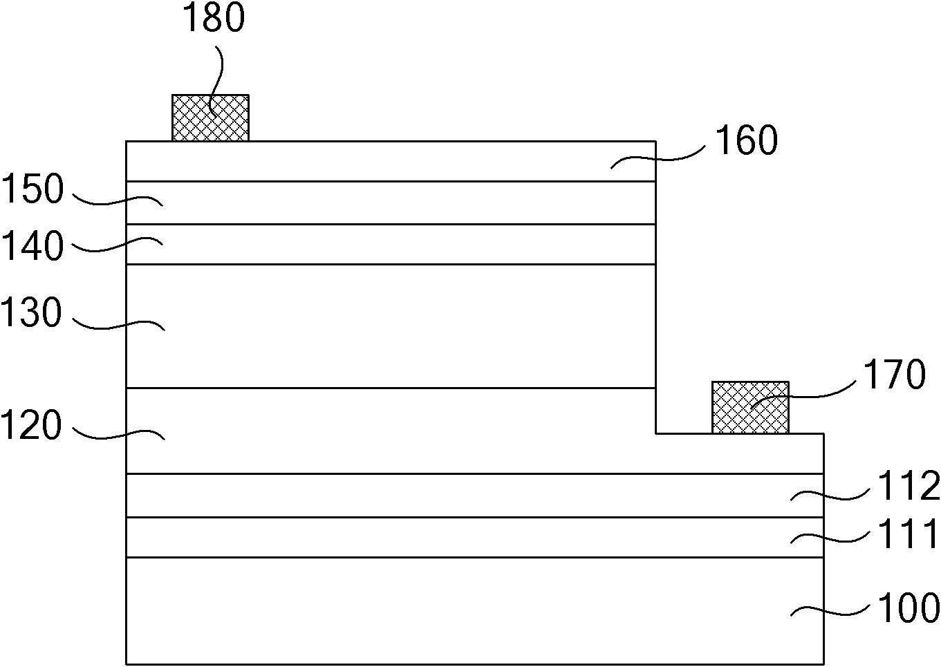
[0030] Please refer to figure 1 , Which is a schematic structural diagram of a light emitting diode according to an embodiment of the invention. Here, taking a gallium nitride-based blue light diode as an example, the light emitting diode includes: a substrate 100; an n-type semiconductor layer 120, an active layer 130, a p-type semiconductor layer 140, and an insert Layer 150 and current spreading layer 160.

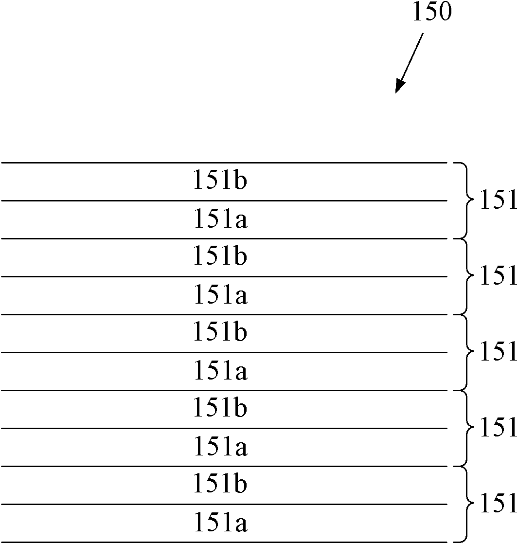
[0031] Such as figure 2 As shown...


PUM

PropertyMeasurementUnit
Thicknessaaaaaaaaaa

Abstract

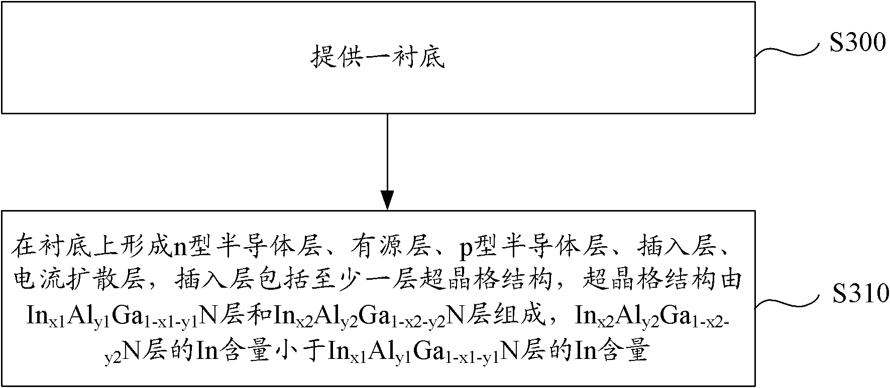
The invention discloses a light-emitting diode and a manufacturing method thereof. The light-emitting diode comprises a substrate, an n type semiconductor layer, an active layer, a p type semiconductor layer, an insertion layer and a current diffusion layer, wherein the n type semiconductor layer, the active layer, the p type semiconductor layer, the insertion layer and the current diffusion layer are sequentially positioned on the substrate; the insertion layer comprises at least one layer of superlattice structure; the superlattice structure consists of an Inx1Aly1Ga1-x1-y1N layer and an Inx2Aly2Ga1-x2-y2N layer; and the In content of the Inx2Aly2Ga1-x2-y2N layer is less than the In content of the Inx1Aly1Ga1-x1-y1N layer. Because the superlattice structure has a certain buffering effect on carrier mobility and a carrier can be effectively tunneled, current is re-distributed in the contact face between a current diffusion layer and the insertion layer, and in the insertion layer and then the current is prevented from being congested. Because the insertion layer has a certain tunneling effect, a forward voltage is not obviously increased. At the same time, because the insertion layer plays a role of buffering on the current between the p type semiconductor layer and the current diffusion layer, the electro-static discharge (ESD) performance of the device is increased.

Description

Technical field [0001] The present invention relates to the field of semiconductor light emitting, in particular to a light emitting diode and a manufacturing method thereof. Background technique [0002] Light Emitting Diodes (LEDs) are used in various fields due to their advantages such as long life and low energy consumption. Especially as their lighting performance indicators are greatly improved, LEDs are often used as light-emitting devices in the lighting field. Among them, III-V compound semiconductors represented by gallium nitride (GaN) have the characteristics of wide band gap, high luminous efficiency, high electronic saturation drift speed, and stable chemical properties. They are used in high-brightness blue light emitting diodes, blue lasers, etc. The field of optoelectronic devices has huge application potential and has attracted widespread attention. At present, the general LED structure uses a p-type semiconductor layer (usually a p-type nitride such as p-type ...

Claims


Application Information

Patent Timeline
IPC IPC(8): H01L33/02H01L33/04H01L33/14H01L33/00
Inventor 李淼
Owner ENRAYTEK OPTOELECTRONICS
Learn More