Semiconductor structure and manufacturing method thereof

A manufacturing method and semiconductor technology, which is applied in semiconductor/solid-state device manufacturing, semiconductor devices, transistors, etc., can solve the problems of semiconductor device electrical performance degradation and achieve the effect of optimizing electrical performance and avoiding loss

Active Publication Date: 2017-11-14
SEMICON MFG INT (SHANGHAI) CORP +1
View PDF5 Cites 15 Cited by
  • Summary
  • Abstract
  • Description
  • Claims
  • Application Information

AI Technical Summary

Problems solved by technology

[0004] However, the shallow trench isolation structure of the prior art is likely to cause the reduction of the electrical performance of the semiconductor device

Method used


Image

  • Semiconductor structure and manufacturing method thereof
  • Semiconductor structure and manufacturing method thereof
  • Semiconductor structure and manufacturing method thereof

Examples


Embodiment Construction

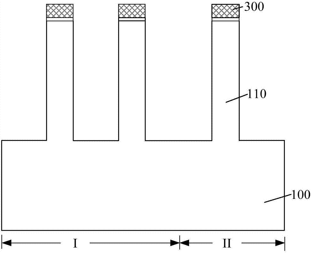
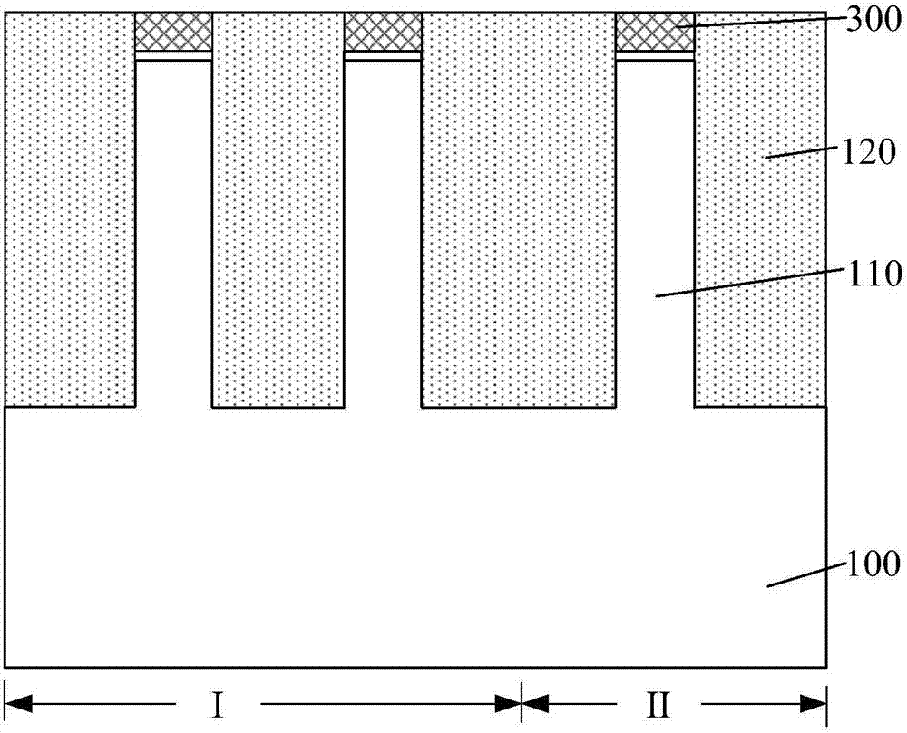
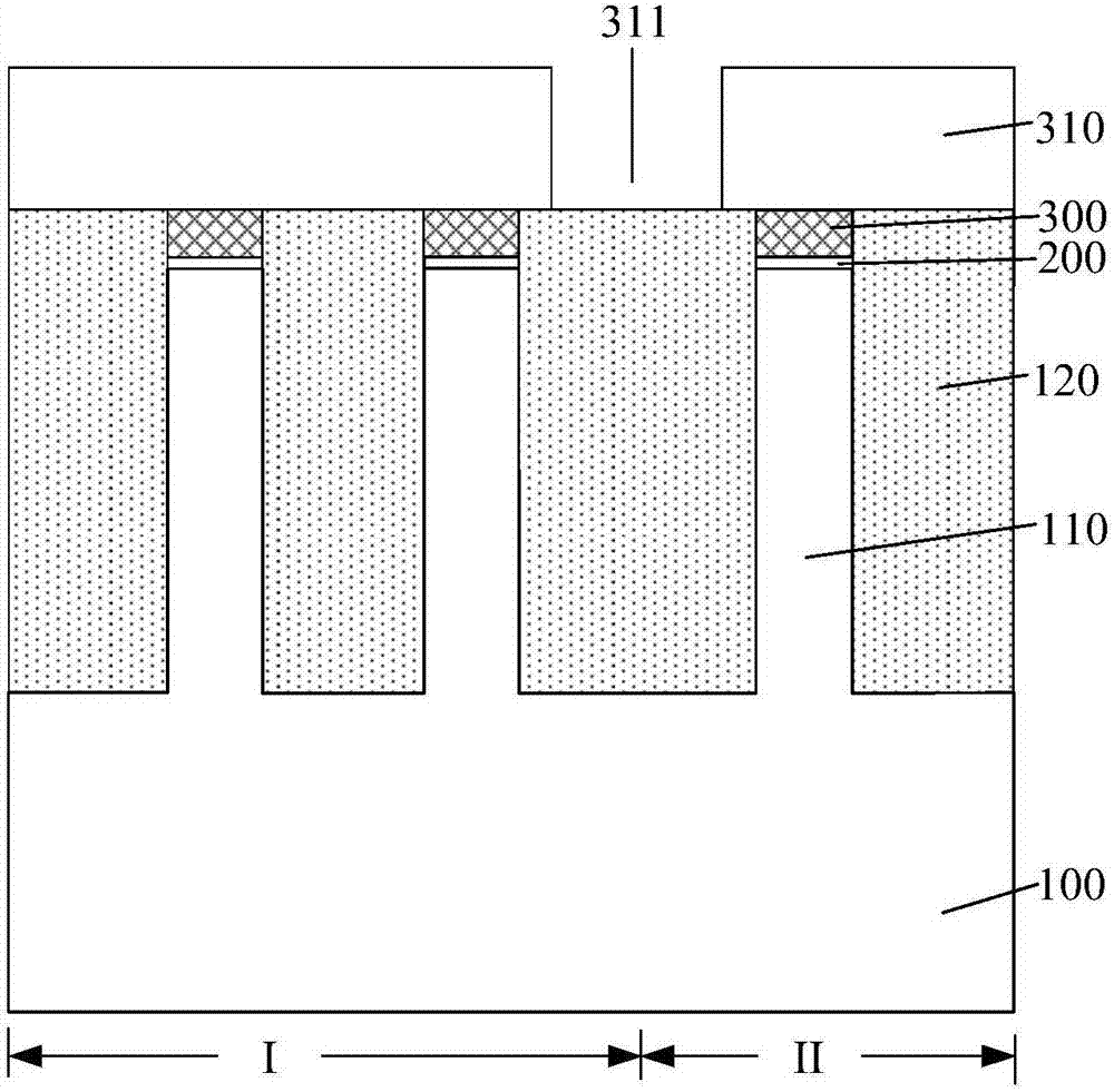
[0031] It can be known from the background technology that the shallow trench isolation structure of the prior art is likely to cause a reduction in the electrical performance of the semiconductor device, and the reason is analyzed in combination with the manufacturing method of the prior art semiconductor structure. Combined reference Figure 1 to Figure 6 , Shows a schematic structural diagram corresponding to each step in an embodiment of a manufacturing method of a prior art semiconductor structure.

[0032] reference figure 1 , Provide a base (not labeled), the base includes a substrate 100 and a fin 110 protruding from the substrate 100, the substrate includes a first area I and a second area II.

[0033] In this embodiment, the substrate is used to form SRAM, the first region I is used to form pull-down (PD, Pull Down) transistors or pass gate (PG, Pass Gate) transistors, and the second region II is used to form Pull up (PU, Pull Up) transistor.

[0034] It should be noted t...


PUM


Abstract

The invention provides a semiconductor structure and a manufacturing method thereof. The manufacturing method comprises the steps of: providing a base which comprises a substrate and fin portions protruding out of the substrate, wherein the substrate comprises a first region and a second region; forming a first initial isolating layer on the substrate; patterning the first initial isolating layer, and forming a first opening through which the substrate is exposed in a junction of the first region and the second region; forming a side wall protective layer which is made of a material different from that of the substrate and the fin portions on the side wall of the first opening; etching the substrate along the first opening, and forming a second opening in the substrate; forming a second initial isolating layer which fills up the second opening and the first opening; and removing a partial thickness of the second initial isolating layer, the side wall protective layer and the first initial isolating layer, so as to expose the fin portions. According to the semiconductor structure and the manufacturing method thereof, the first opening is formed in the first initial isolating layer at first, then the side wall protective layer is formed on the side wall of the first opening, and the substrate is etched along the first opening; and the side wall protective layer can protect the fin portions on two sides of the first opening, thereby preventing the fin portions from being damaged by the process of etching the substrate.

Description

Technical field [0001] The present invention relates to the field of semiconductors, in particular to a semiconductor structure and a manufacturing method thereof. Background technique [0002] With the development trend of high density of integrated circuits, the devices that make up the circuit are placed more closely in the chip to fit the available space of the chip. Correspondingly, the density of active devices per unit area of ​​a semiconductor substrate is increasing, so effective insulation between devices becomes more important. [0003] Shallow Trench Isolation (STI) technology has a good isolation effect (for example: process isolation effect and electrical isolation effect), shallow trench isolation technology also reduces the area occupied on the wafer surface and increases the integration of devices Etc. Therefore, with the reduction in the size of integrated circuits, the isolation between devices now mainly adopts a shallow trench isolation structure. [0004] How...

Claims


Application Information

Patent Timeline
Patent Type & Authority Applications(China)
IPC IPC(8): H01L21/762H01L21/8244H01L27/11
CPCH01L21/76224H10B10/12
Inventor 周飞
Owner SEMICON MFG INT (SHANGHAI) CORP
Why Eureka
Try Eureka