Three-dimensional multilayer waveguide mode multiplexing and de-multiplexing device and preparation method thereof

A mode multiplexing, three-dimensional multi-layer technology, applied in the direction of optical waveguide light guide, light guide, instrument, etc., can solve the problems such as inability to directly couple, and achieve the goal of increasing device integration dimension, increasing integration degree, improving device integration degree and flexibility Effect

Pending Publication Date: 2018-11-06
NANJING UNIV OF POSTS & TELECOMM
View PDF0 Cites 14 Cited by
  • Summary
  • Abstract
  • Description
  • Claims
  • Application Information

AI Technical Summary

Problems solved by technology

Direct three-dimensional coupling of modes is achieved by aligning the boundaries of either side of the upper and lower waveguides, which overcomes the defect that traditional devices cannot be directly coupled and additional devices need to be added

Method used


Image

  • Three-dimensional multilayer waveguide mode multiplexing and de-multiplexing device and preparation method thereof
  • Three-dimensional multilayer waveguide mode multiplexing and de-multiplexing device and preparation method thereof
  • Three-dimensional multilayer waveguide mode multiplexing and de-multiplexing device and preparation method thereof

Examples


preparation example Construction

[0051] A method for preparing the three-dimensional waveguide mode multiplexer and demultiplexer, comprising the following steps:

[0052] Step 1: Take a piece of silicon substrate, treat the surface of the silicon wafer, and deposit a 2-3 μm silicon dioxide cladding layer on the surface of the silicon substrate by chemical vapor deposition (PECVD), which is the lower cladding layer. The reaction gas for the deposition of silicon dioxide is silane (SiH 4 ) and nitric oxide (N 2 O). During the deposition process, the temperature of the upper plate is 300°C, the temperature of the lower plate is 300°C, the power of the RF source is 700W, the cavity pressure is 300mTorr, N 2 O flow is 2000sccm, SiH 4 The flow rate is 17sccm,

[0053] Step 2: Carry out uniform photolithography on the lower cladding layer, and spread the photoresist on the surface of the chip at a low speed. The typical low speed speed is 1500-1750r / min, 3-5s; after that, the high speed volatilizes the photores...

Embodiment 1

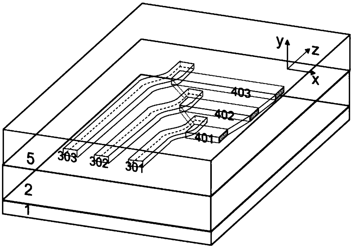
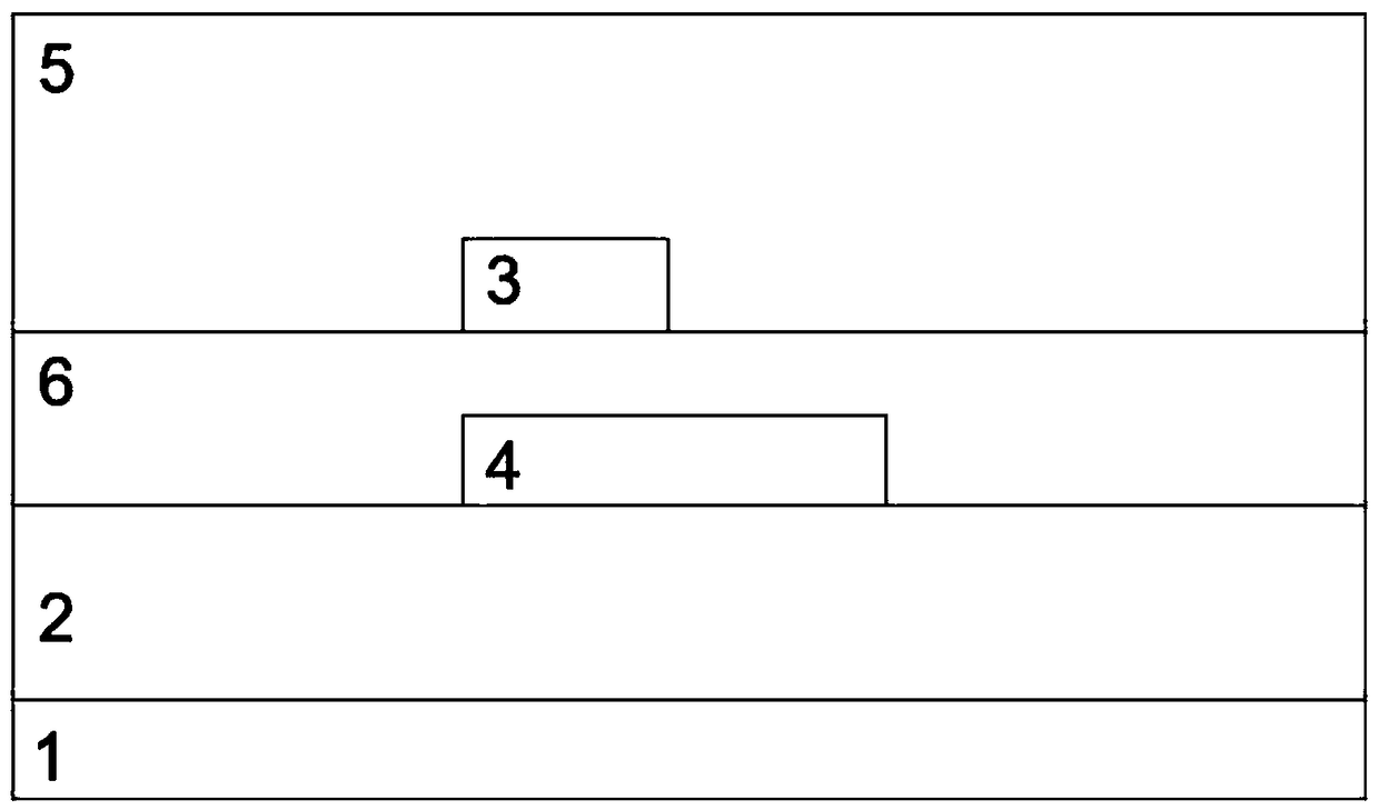
[0063] refer to figure 2 As shown, a three-dimensional multilayer waveguide mode multiplexer and demultiplexer includes a substrate layer 1, a lower cladding layer 2, an upper waveguide 3, a lower waveguide 4, an upper cladding layer 5 and an intermediate isolation layer 6.

[0064] figure 2 In the three-dimensional multi-layer waveguide mode multiplexer and demultiplexer shown, the lower layer waveguide 4 has a gradually changing width structure, including the first trunk waveguide section 401, the second trunk waveguide section 402 and the third trunk waveguide section 403, which can realize Multiplexing and demultiplexing of different high-order modes; the upper waveguide 3 includes a first input waveguide 301 , a second input waveguide 302 and a third input waveguide 303 .

[0065] Through the construction of a three-dimensional multilayer waveguide structure, compared with the traditional two-dimensional planar waveguide mode multiplexer and demultiplexer structure, th...

Embodiment 2

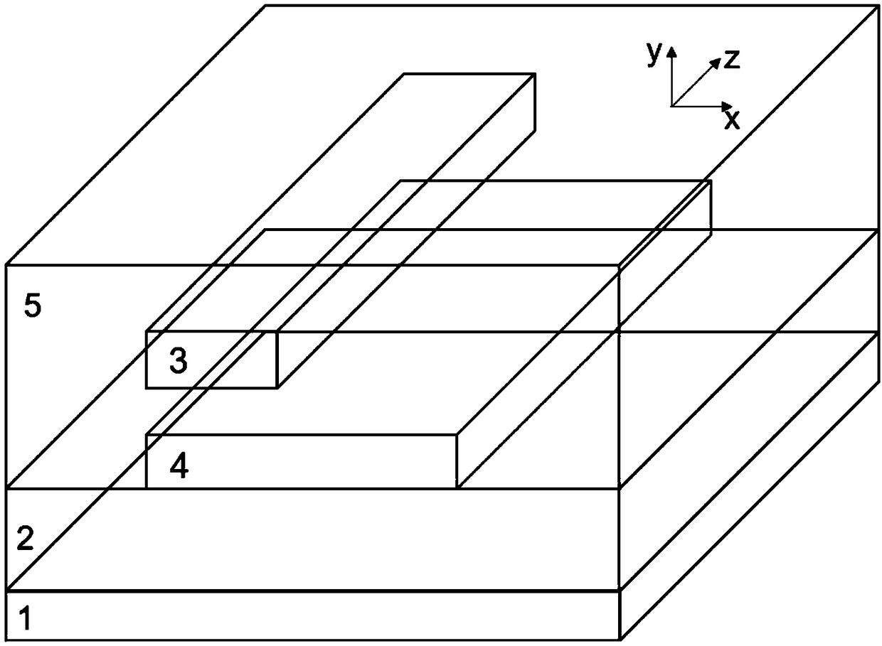
[0067] refer to image 3As shown, a three-dimensional multilayer waveguide retest multiplexer and demultiplexer includes a substrate layer 1, a lower cladding layer 2, an upper waveguide 3, a lower waveguide 4, an upper cladding layer 5 and an intermediate isolation layer 6.

[0068] image 3 The three-dimensional multi-layer waveguide single-mode multiplexer and demultiplexer shown is an example of analysis of a specific situation. In this structure, both the lower trunk waveguide and the upper layer input waveguide have only a section of structure, which belongs to the partial situation in the first embodiment. The specific analysis . The width h of the upper and lower waveguides is the same, both are 220nm, and the width of the lower waveguide w 1 =838nm, upper layer waveguide width w 2 =400nm, the gap between the upper and lower waveguides Gap=200nm. The upper layer waveguide 3 adopts a P-type silicon waveguide, and the lower layer waveguide 4 adopts a silicon waveguid...


PUM


Abstract

The invention relates to a three-dimensional multilayer waveguide mode multiplexing and de-multiplexing device and a preparation method thereof and belongs to the optical communication device technical field, in particular, a mode division multiplexing system. According to the three-dimensional multilayer waveguide mode multiplexing and de-multiplexing device and the preparation method thereof ofthe invention, a three-dimensional multilayer waveguide integrated structure is adopted, and therefore, the limitations of a traditional two-dimensional planar waveguide structure can be eliminated, the integration dimensions of the device can be increased, the integration and flexibility of the device can be enhanced, and the communication capacity of a system can be improved. The boundary of anyone side of the upper-layer waveguide of the three-dimensional waveguide is aligned with the boundary of any one side of the lower-layer waveguide of the three-dimensional waveguide, so that the direct three-dimensional coupling of a fundamental mode and a high-order mode is realized, and therefore, a defect that a traditional three-dimensional mode multiplexer fails to realize direct coupling ofmodes can be eliminated, and the structure and complexity of the device can be simplified. The device of the invention is prepared based on a mature CMOS process, so that high efficiency, low cost and mass production of the device can be realized. With the three-dimensional multilayer waveguide mode multiplexing and de-multiplexing device and the preparation method thereof of the invention adopted, the flexible three-dimensional coupling of the modes can be realized, a solid foundation is laid for on-chip mode multiplexing technology. The three-dimensional multilayer waveguide mode multiplexing and de-multiplexing device and the preparation method thereof can be further applied to the flexible mode routing of a mode division multiplexing network.

Description

technical field [0001] The invention relates to a three-dimensional multilayer waveguide mode multiplexer and demultiplexer and a preparation method, belongs to the technical field of optical communication devices, and is specifically aimed at a mode division multiplex system. Background technique [0002] With the rapid development of the communication industry, the era of big data provides higher requirements for the transmission of communication networks, and people's demand for bandwidth capacity is increasing day by day. The most widely used in traditional optical communication systems is Waveguide-division multiplexing (WDM). But nowadays, people are faced with the serious problem that the bandwidth demand far exceeds the bandwidth capacity that the WDM technology can provide, thus, the mode-division multiplexing technology (Mode-division multiplexing, MDM) has gained people's attention. [0003] MDM technology, using different modes in optical fiber or waveguide to r...

Claims


Application Information

Patent Timeline
Patent Type & Authority Applications(China)
IPC IPC(8): G02B6/12G02B6/132G02B6/138
CPCG02B6/12007G02B6/12002G02B6/132G02B6/138
Inventor 蒋卫锋程方圆许吉万洪丹
Owner NANJING UNIV OF POSTS & TELECOMM
Why Eureka
Try Eureka