
Method for fabricating metal gate structure

a gate structure and metal technology, applied in the direction of basic electric elements, electrical apparatus, semiconductor devices, etc., can solve the problems of reducing the gate capacitance, worsening the driving ability of the device, and affecting the performance of the device, so as to improve the oxygen content of the hk dielectric layer, reduce the oxygen content of the titanium nitride layer, and improve the driving ability.

Active Publication Date: 2018-07-05
UNITED MICROELECTRONICS CORP
View PDF4 Cites 5 Cited by
  • Summary
  • Abstract
  • Description
  • Claims
  • Application Information

AI Technical Summary

Benefits of technology

The invention provides a method for making a metal gate structure that can reduce NBTI and increase its lifetime. The method achieves this by reducing the oxygen content in the oxygen-containing titanium nitride layer and increasing it in the HK dielectric layer and the amorphous silicon layer. This improves the quality of both the titanium nitride layer and the dielectric layer, ultimately lifting the metal gate structure.

Problems solved by technology

With the trend towards scaling down the size of the MOS transistor, conventional poly-silicon gates face problems such as inferior performances due to boron penetration and unavoidable depletion effect, which increases the equivalent thickness of the gate dielectric layer, reduces the gate capacitance, and worsens a driving ability of the device.
However, when the semiconductor technology is scaled down to the nano-scale, the thickness of the HK dielectric layer is more and more thin.
Accordingly, the work function metal gate structure gradually reaches its physical and electrical limits, and so reliability problem of negative bias temperature instability is more and more serious, thereby shrinking the lifetime of the semiconductor device.

Method used


Image

  • Method for fabricating metal gate structure
  • Method for fabricating metal gate structure
  • Method for fabricating metal gate structure

Examples


Embodiment Construction

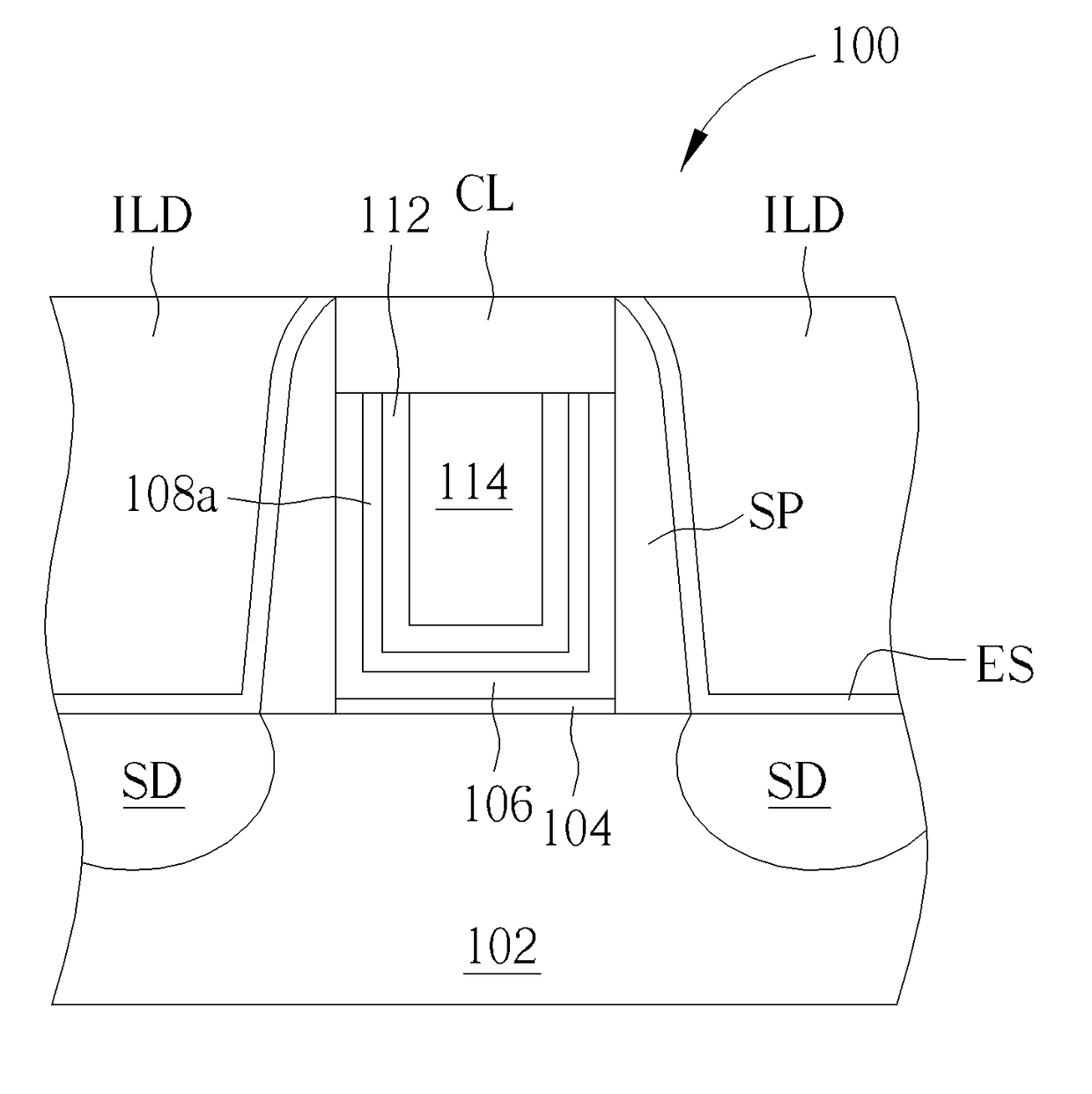
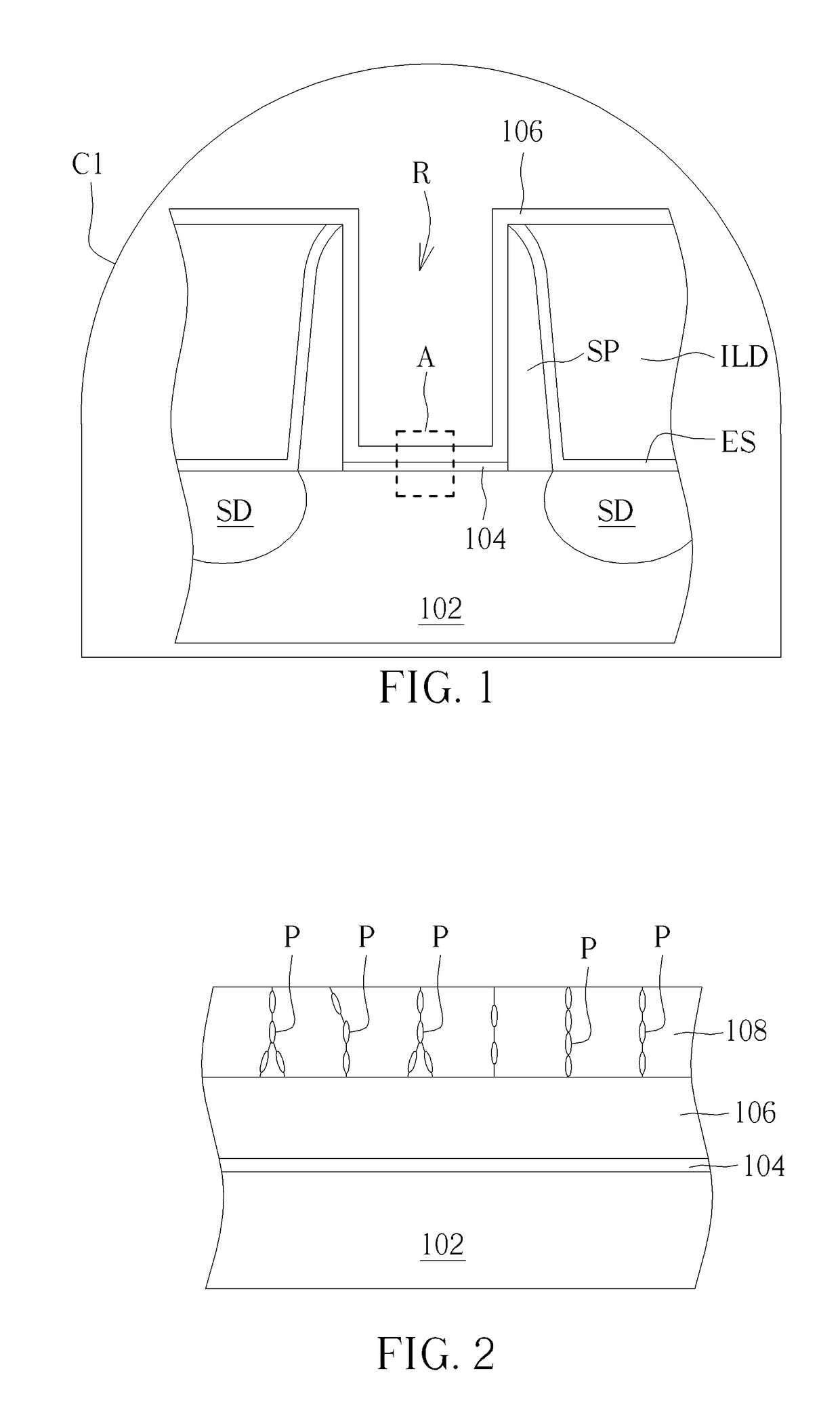
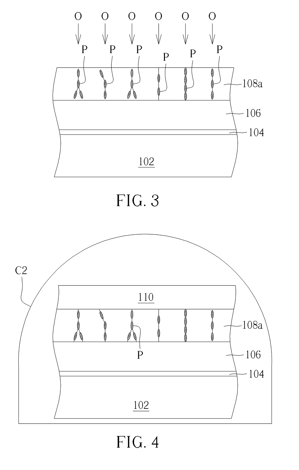
[0009]Refer to FIGS. 1-7, which are schematic diagrams illustrating a method for fabricating a metal gate structure according to an embodiment of the present invention, in which FIGS. 2-6 illustrate different steps corresponding to region A shown in FIG. 1 respectively. As shown in FIG. 1, a substrate 102 is provided first, which includes a semiconductor substrate, such as a silicon substrate, a silicon-containing substrate, a III-V compound semiconductor on silicon substrate, such as GaN-on-silicon substrate, a graphene-on-silicon substrate or a silicon-on-insulator (SOI) substrate. In this embodiment, the substrate 102 may have a dummy gate, two spacers SP, an etching stop layer ES and inter-layer dielectric layer ILD formed thereon. For example, the substrate 102 may include a fin structure, but not limited thereto. After removing the dummy gate between the spacers SP, there is a recess R between the spacers SP which exposes the substrate 102. The dummy gate may include polysilic...


PUM

PropertyMeasurementUnit
thicknessaaaaaaaaaa
temperatureaaaaaaaaaa
thicknessaaaaaaaaaa

Abstract

A method for fabricating a metal gate structure includes following steps. A substrate is provided and followed by forming a high-K dielectric layer on the substrate. Then, an oxygen-containing titanium nitride layer is formed on the high-K dielectric layer. Next, an amorphous silicon layer is formed on the oxygen-containing titanium nitride layer and followed by performing an annealing process to drive oxygen in the oxygen-containing titanium nitride layer to the high-K dielectric layer.

Description

BACKGROUND OF THE INVENTION1. Field of the Invention[0001]The present invention relates to a method for fabricating a metal gate structure, and more particularly, to a method for fabricating a metal gate structure to mitigate negative bias temperature instability (NBTI).2. Description of the Prior Art[0002]In conventional semiconductor technology, poly-silicon is used as a gate electrode so as to be widely applied in semiconductor devices, such as the metal-oxide-semiconductor(MOS) transistors. With the trend towards scaling down the size of the MOS transistor, conventional poly-silicon gates face problems such as inferior performances due to boron penetration and unavoidable depletion effect, which increases the equivalent thickness of the gate dielectric layer, reduces the gate capacitance, and worsens a driving ability of the device. Therefore, work function metals are used as a new gate material to replace the conventional poly-silicon gate to be worked with new high-K(HK) diele...

Claims


Application Information

Patent Timeline
Patent Type & Authority Applications(United States)
IPC IPC(8): H01L21/28
CPCH01L21/28185H01L21/28088H01L21/02326H01L29/495H01L29/518H01L29/517H01L29/4966H01L29/515H01L21/02323
Inventor CHEN, SHAO-PING
Owner UNITED MICROELECTRONICS CORP
Learn More