Capacitor structure

Inactive Publication Date: 2007-08-09
UNITED MICROELECTRONICS CORP
View PDF14 Cites 38 Cited by
  • Summary
  • Abstract
  • Description
  • Claims
  • Application Information

AI Technical Summary

Benefits of technology

[0009] According to another aspect of the present invention, a capacitor structure is provided which can prevent bridge effect between various conductive

Problems solved by technology

Wherein, the MIM capacitor and the MOM capacitor are widely used in deep sub-micron ICs, however, the unit area capacitance thereof is low.
In addition, if the material with high dielectric constant is used, even though high capacitance density can be achiev

Method used


Image

  • Capacitor structure
  • Capacitor structure
  • Capacitor structure

Examples


Example

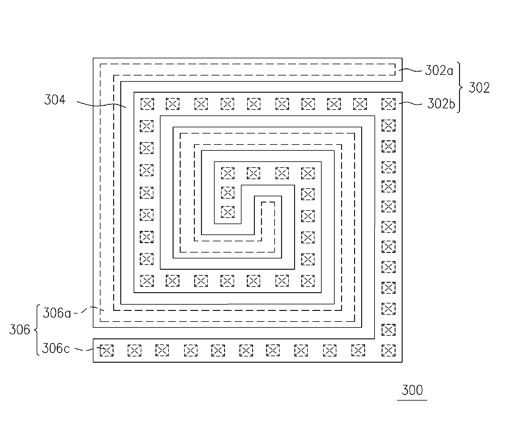
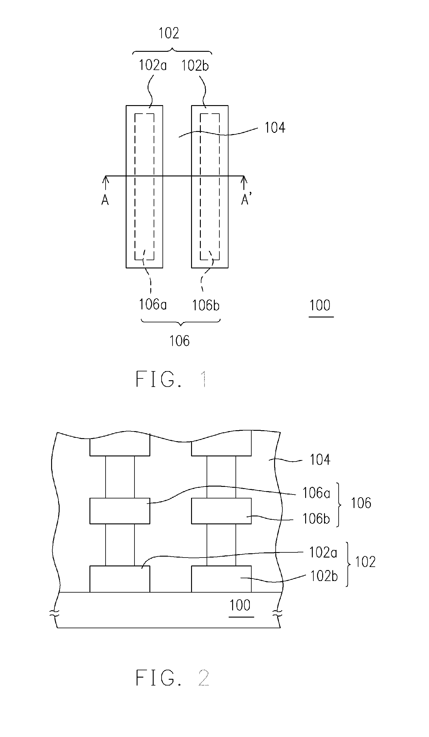
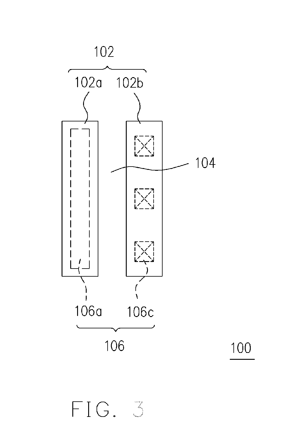
[0041]FIG. 1 is a top view of a capacitor structure according to an embodiment of the present invention. FIG. 2 is a profile view of the capacitor structure cut along line A-A′ in FIG. 1. FIG. 3 is a top view of a capacitor structure according to another embodiment of the present invention.

[0042] First, referring to FIG. 1 and FIG. 2, the capacitor structure includes a plurality of conductive layers 102, a dielectric layer 104, and a plurality of contacts 106 disposed on a substrate 100. The substrate 100 is, for example, a silicon substrate.

[0043] The conductive layers 102 are stacked, and each conductive layer 102 has a conductive pattern 102a and a conductive pattern 102b. The material of the conductive layers 102 is conductive material such as metal. Here, the plurality of the conductive layers 102 means that at least 2 layers are included. For those of ordinary skill in the art, the number of the conductive layers 102 can be adjusted according to the requirement in IC design....


PUM


Abstract

A capacitor structure including a plurality of conductive layers, a dielectric layer and a plurality of contacts is disclosed. The conductive layers are stacked, and each conductive layer has a first conductive pattern and a second conductive pattern. The dielectric layer is disposed between the first conductive pattern and the second conductive pattern and between two adjacent conductive layers. The contacts are disposed in the dielectric layer, and electrically connected to the first conductive patterns in two adjacent conductive layers and electrically connected to the second conductive patterns in two adjacent conductive layers. Wherein, the contact electrically connecting to the first conductive patterns in two adjacent conducive layers is a first strip contact, which extends between the first conductive patterns in two adjacent conductive layers, and the boundary of the first strip contact is located within the boundary of the first conductive pattern.

Description

BACKGROUND OF THE INVENTION [0001] 1. Field of Invention [0002] The present invention relates to a capacitor structure. More particularly, the present invention relates to a capacitor structure having high unit area capacitance. [0003] 2. Description of Related Art [0004] Capacitor is one of the indispensable elements in an integrated circuit. During the design and fabricating process of a capacitor, the capacitance and allocation area of the capacitor have to be considered, thus a better design and fabricating process for capacitor can be provided. [0005] Generally speaking, capacitors can be divided into 3 categories: metal-insulator-meta (MIM) capacitor, metal-line to metal-line (MOM) capacitor, and metal-insulator-silicon (MIS) capacitor. Wherein, the MIM capacitor and the MOM capacitor are widely used in deep sub-micron ICs, however, the unit area capacitance thereof is low. In addition, if the material with high dielectric constant is used, even though high capacitance density...

Claims


Application Information

Patent Timeline
IPC IPC(8): H01L29/00
CPCH01L23/5223H01L28/60H01L2924/0002H01L2924/00
Inventor HUNG, CHENG-CHOULIANG, VICTORTSENG, HUA-CHOUTSENG, CHIH-YU
Owner UNITED MICROELECTRONICS CORP
Why Eureka
Try Eureka