

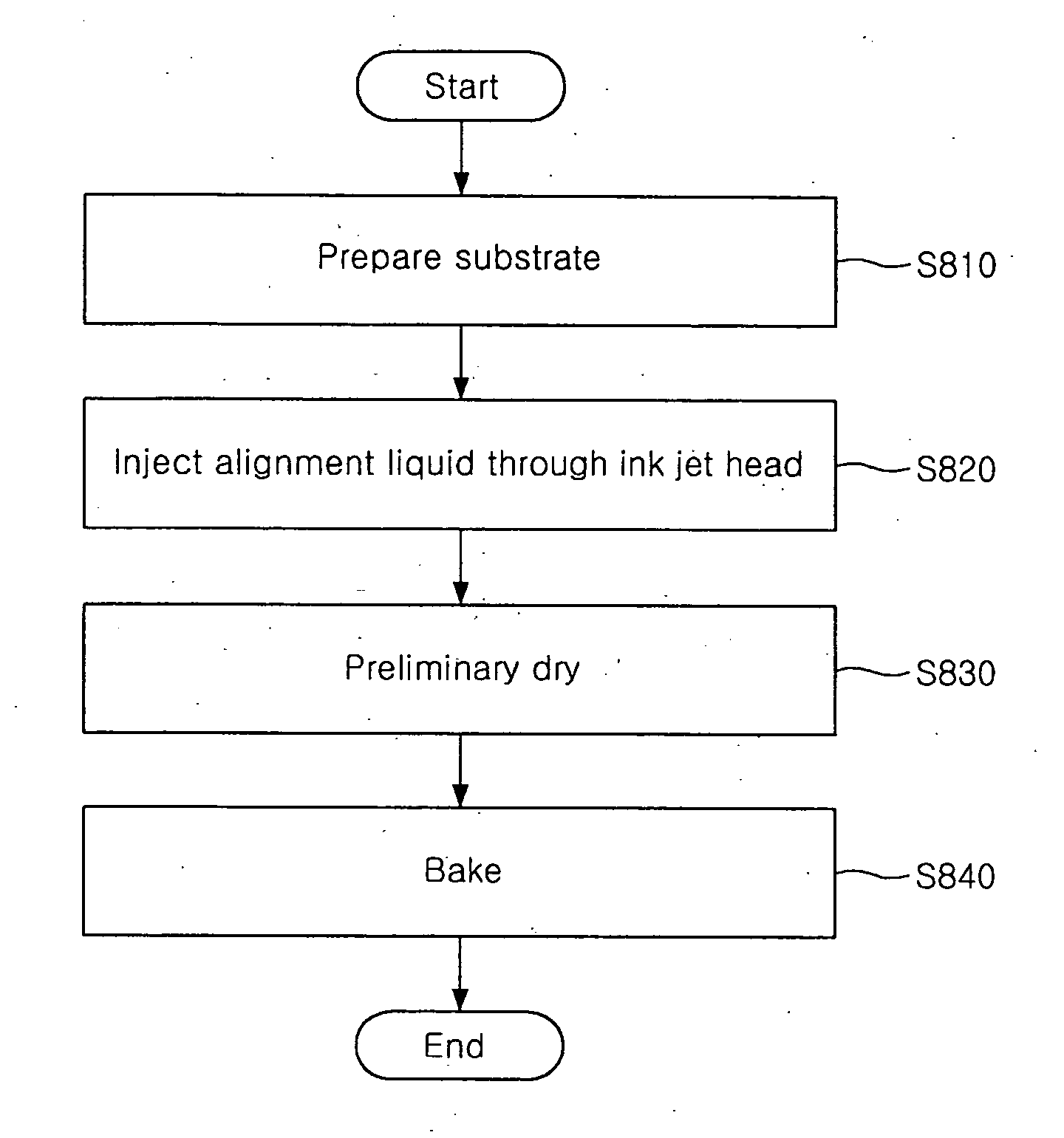
Printing alignment layers on LCD substrates with ink jet printing apparatus
- Summary
- Abstract
- Description
- Claims
- Application Information
AI Technical Summary
Benefits of technology
Problems solved by technology
Method used
Image

Examples
Embodiment Construction
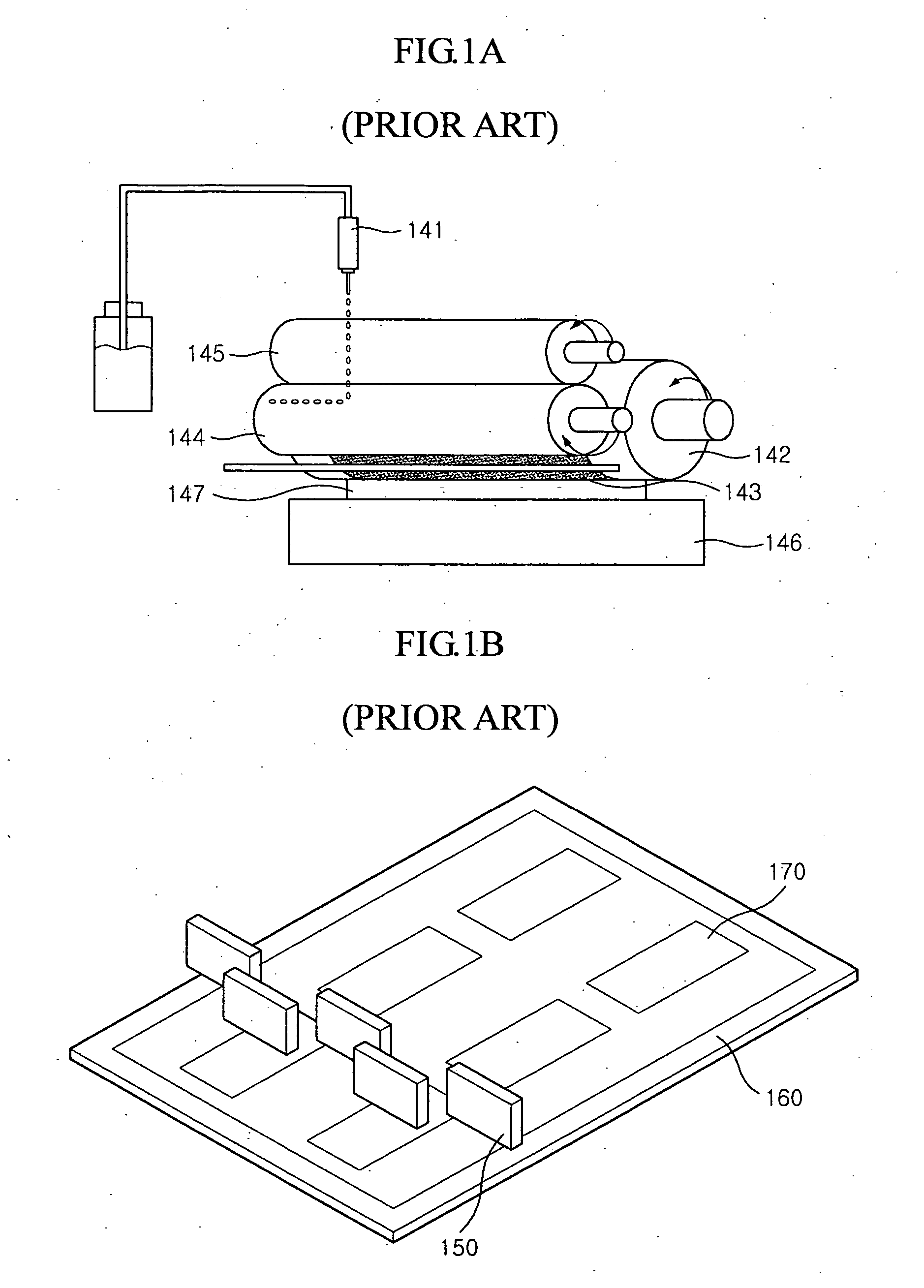
[0028]FIG. 4 is a partial schematic view of an ink jet head of an exemplary embodiment of an alignment layer printing apparatus in accordance with the present invention. As shown in FIG. 4, the ink jet head comprises an orifice unit 400, a plurality of piezoelectric elements 500, an alignment layer ink supply unit 600 and a plurality of potentiometers, or variable resistors 700. In the schematic view of FIG. 4, the variable resistors and the piezoelectric elements are shown in elevation view and mounted on and coupled to each other through a printed circuit board (PCB), whereas, the ink supply unit 600 and the orifice unit are disposed below the piezoelectric elements and shown in partial plan views rotated to lie in the plane of the PCB for illustration purposes.
[0029] As described in more detail below with reference to FIGS. 5A to 6C, the orifice unit 400A contains a plurality of orifices for ejecting an alignment layer ink directly onto an LCD substrate (not illustrated) dispose...
PUM
| Property | Measurement | Unit |
|---|---|---|
| Distance | aaaaa | aaaaa |
| Thickness | aaaaa | aaaaa |
| Angle | aaaaa | aaaaa |
Abstract
Description
Claims
Application Information