Power semiconductor arrangement, power semiconductor module with multiple power semiconductor arrangements, and module assembly comprising multiple power semiconductor modules

Inactive Publication Date: 2013-02-21
ABB TECH AG
View PDF7 Cites 1 Cited by
  • Summary
  • Abstract
  • Description
  • Claims
  • Application Information

AI Technical Summary

Benefits of technology

[0012]An exemplary embodiment of the present disclosure provides a power semiconductor arrangement which includes a base plate having a molybdenum layer. The exemplary power semiconductor arrangement also includes a power semiconductor device mounted to a top side of the base plate and electrically and thermally coupled thereto. In addition, the exemplary power semiconductor arra

Problems solved by technology

In case one of the power semiconductor devices fails, it fails by providing a short circuit to enable conduction from the base plate to the lid.
In this short circuit failure mode, very high currents can flow through a single power semiconductor device, since the short circuit disables all parallel power semiconductor devices.
When the power semiconductor device fails and the short circuit current raises the temperature, the aluminum melts and forms an alloy with the silicon of the power semiconductor device.
Nevertheless, aging of the contact between the base plate and the failed power semiconductor device can increase electrical resistance up to a point that it is high enough to break another power semiconductor device, so that the problem is propagated through the entire power semiconductor module and the entire module assembly.
In the area of power and high power semiconductors, this is of concern, since large amounts of energy are present and arcing can occur within the power semiconductor module.
Worst case, even neighbouring cooler damages can occur or a failure of the entire system.
Investigation ha

Method used


Image

  • Power semiconductor arrangement, power semiconductor module with multiple power semiconductor arrangements, and module assembly comprising multiple power semiconductor modules
  • Power semiconductor arrangement, power semiconductor module with multiple power semiconductor arrangements, and module assembly comprising multiple power semiconductor modules

Examples


Example

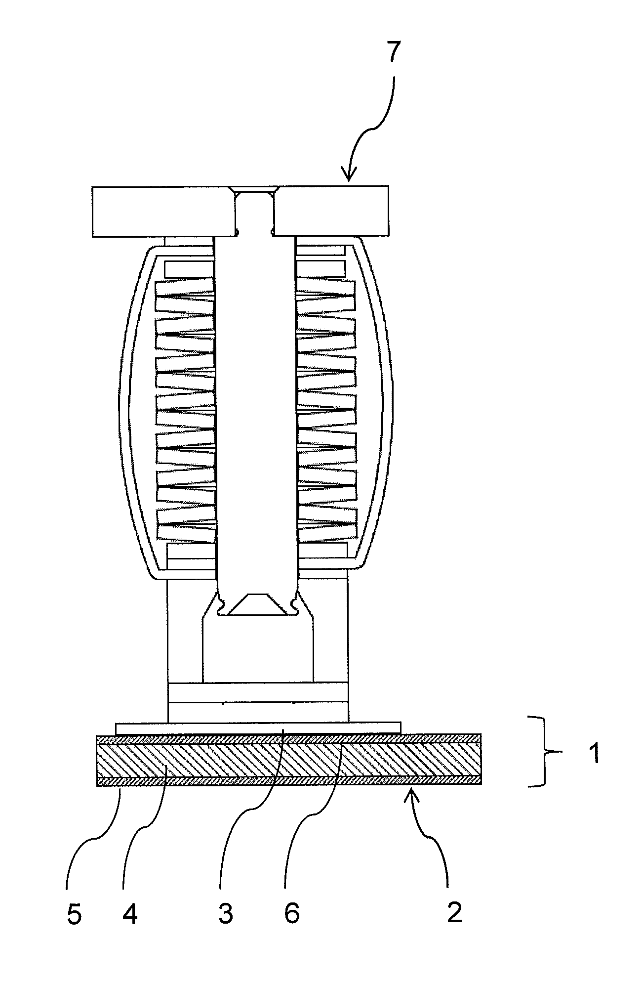
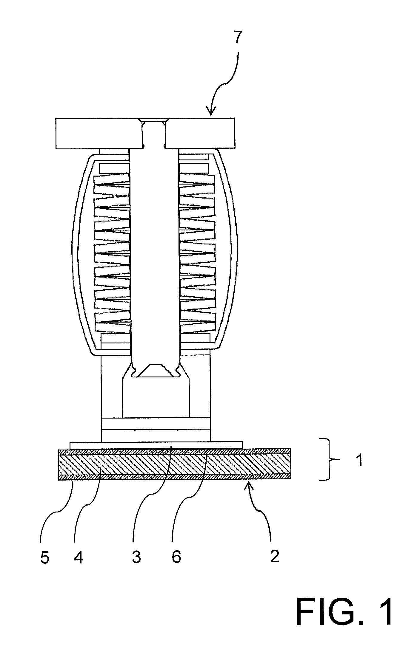
[0015]Exemplary embodiments of the present disclosure provide a power semiconductor arrangement, a power semiconductor module with multiple power semiconductor arrangements, and a module assembly including multiple power semiconductor modules, which have a long lifetime of the electrical and thermal connection between the power semiconductor device and the base plate and provide good heat transfer away from the power semiconductor device, such as in a short circuit failure mode.

[0016]An exemplary embodiment of the present disclosure provides a power semiconductor arrangement, which includes a base plate having a molybdenum layer, and a power semiconductor device mounted to a top side of the base plate and electrically and thermally coupled thereto. The base plate includes a metallic mounting base, which is arranged between the semiconductor device and the molybdenum layer and prevents the molybdenum layer from forming highly resistive intermetallic phases with the semiconductor devi...


PUM


Abstract

A power semiconductor arrangement includes a base plate having a molybdenum layer, and a power semiconductor device mounted to a top side of the base plate and electrically and thermally coupled thereto. The base plate includes a metallic mounting base, which is arranged between the semiconductor device and the molybdenum layer and prevents the molybdenum layer from forming highly resistive intermetallic phases with the semiconductor device. A semiconductor module, such as a power semiconductor module, includes multiple semiconductor arrangements, whereby the base plate of the semiconductor arrangements is a common base plate. A module assembly, such as a power semiconductor module assembly, includes multiple semiconductor modules, whereby the semiconductor modules are arranged side by side to each other with electric connections between adjacent semiconductor modules.

Description

RELATED APPLICATION[0001]This application claims priority under 35 U.S.C. §119 to European Patent Application No. 11177801.5 filed in Europe on Aug. 17, 2011, the entire content of which is hereby incorporated by reference in its entirety.FIELD[0002]The present disclosure relates to a power semiconductor arrangement, which includes a base plate having a molybdenum layer, and a power semiconductor device mounted to a top side of the base plate and electrically and thermally coupled thereto. The present disclosure also relates to a power semiconductor module with multiple power semiconductor arrangements. The present disclosure also relates to a module assembly, such as a power semiconductor module assembly, including multiple power semiconductor modules.BACKGROUND INFORMATION[0003]Power semiconductor arrangements of the aforementioned kind are known in the art and are used, for example, in the area of mounting and contacting power semiconductor devices as well as high power semicondu...

Claims


Application Information

Patent Timeline
IPC IPC(8): H01L23/06
CPCH01L23/051H01L23/4924H01L23/62H01L24/72H01L25/072H01L2924/01327H01L2924/13055H01L2924/1305H01L2924/15763H01L2924/00H01L23/12
Inventor DUGAL, FRANC
Owner ABB TECH AG
Why Eureka
Try Eureka