

Offset correction during correlated double sampling in CMOS image sensor
- Summary
- Abstract
- Description
- Claims
- Application Information
AI Technical Summary
Benefits of technology
Problems solved by technology
Method used
Image

Examples
Embodiment Construction
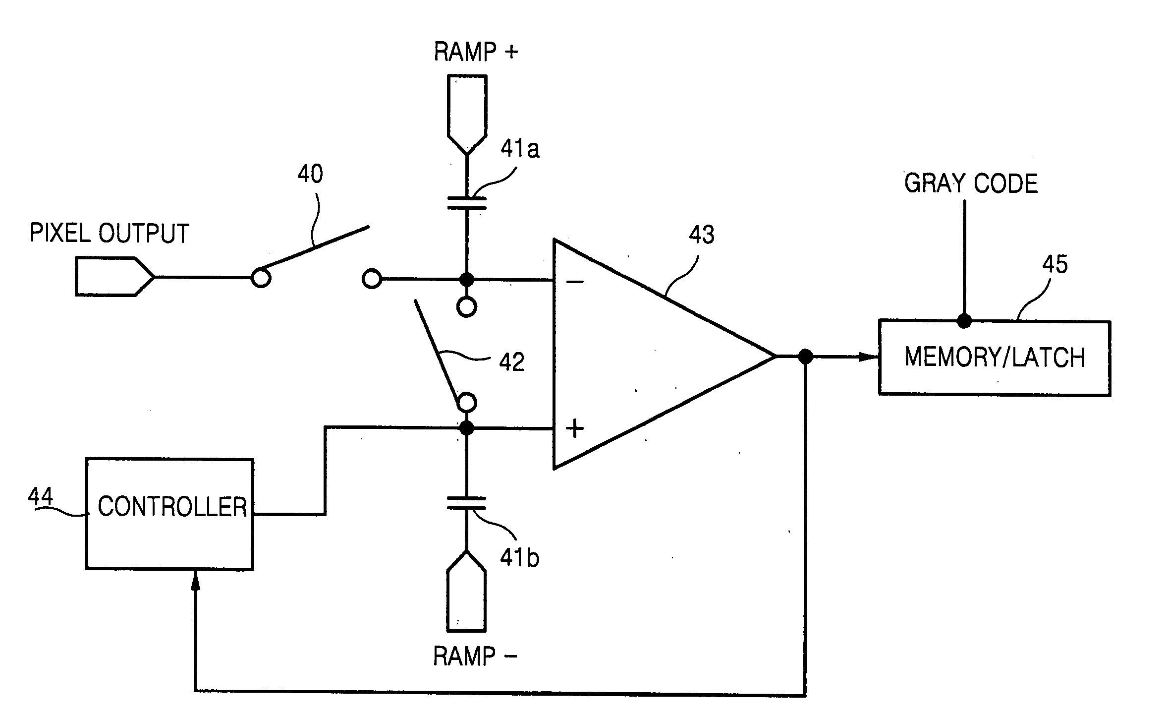
[0043]FIG. 4 illustrates an apparatus for correlated double sampling (CDS) / analog-to-digital conversion (ADC) within a CMOS image sensor according to an embodiment of the present invention. Referring to FIG. 4, the CDS / ADC apparatus includes a comparator 43, a first capacitor 41a, a second capacitor 41b, a first switch 40, a second switch 42, a controller 44, and a memory / latch unit 45.
[0044]The comparator 43 sequentially receives a reset voltage and a sensing voltage from a pixel at a positive (+) input terminal and a negative (−) input terminal. The first capacitor 41a has a first end coupled to the negative (−) input of the comparator 43 and has a second end having a positive ramp voltage RAMP+ applied thereon. The second capacitor 41b has a first end coupled to the positive (+) input of the comparator 43 and has a second end having a negative ramp voltage RAMP− applied thereon.
[0045]The first switch 40 is coupled between the first end of the first capacitor 41a and an output ter...
PUM
 Abstract
Description
Claims
Application Information