A switch bootstrap charging circuit suitable for high-speed gate driving of GaN power device

A technology of power devices and charging circuits, applied in the field of switching bootstrap charging circuits, can solve the problems of inability to apply to high-frequency applications, inability to achieve full integration, and high voltage, and achieve high reliability, small cost and area, and simple circuit structure. Effect

Active Publication Date: 2018-12-14
UNIV OF ELECTRONICS SCI & TECH OF CHINA
View PDF10 Cites 12 Cited by
  • Summary
  • Abstract
  • Description
  • Claims
  • Application Information

AI Technical Summary

Problems solved by technology

[0005] Aiming at the disadvantages that the above-mentioned traditional bootstrap charging circuit cannot be applied to the gate drive of GaN power devices because the voltage on the bootstrap capacitor Cboot is too high during the dead time, cannot be fully integrated and cannot be applied to high-frequency applications, the present invention A switch bootstrap charging circuit is proposed, which controls the opening of the bootstrap charging path through a double-switch structure, avoiding the bootstrap charging circuit from charging the bootstrap capacitor Cboot in the dead time, thereby preventing the problem of excessive voltage on the bootstrap capacitor Cboot; At the same time, the high-voltage switching device is used to replace the function of the bootstrap diode Dboot in the traditional bootstrap charging circuit, and the circuit is completely integrated on the chip. There is no reverse recovery time limit of the diode, and it can work at a higher frequency, and there is no reverse recovery current and reverse recovery. The additional loss caused by the recovery; it can effectively prevent the circuit from being affected by the crosstalk when the chip switch is switched, and the invention is especially suitable for high-speed gate drive of GaN power devices

Method used


Image

  • A switch bootstrap charging circuit suitable for high-speed gate driving of GaN power device
  • A switch bootstrap charging circuit suitable for high-speed gate driving of GaN power device
  • A switch bootstrap charging circuit suitable for high-speed gate driving of GaN power device

Examples


Embodiment Construction

[0020] The technical solution of the present invention will be described in detail below in conjunction with the accompanying drawings and specific embodiments.

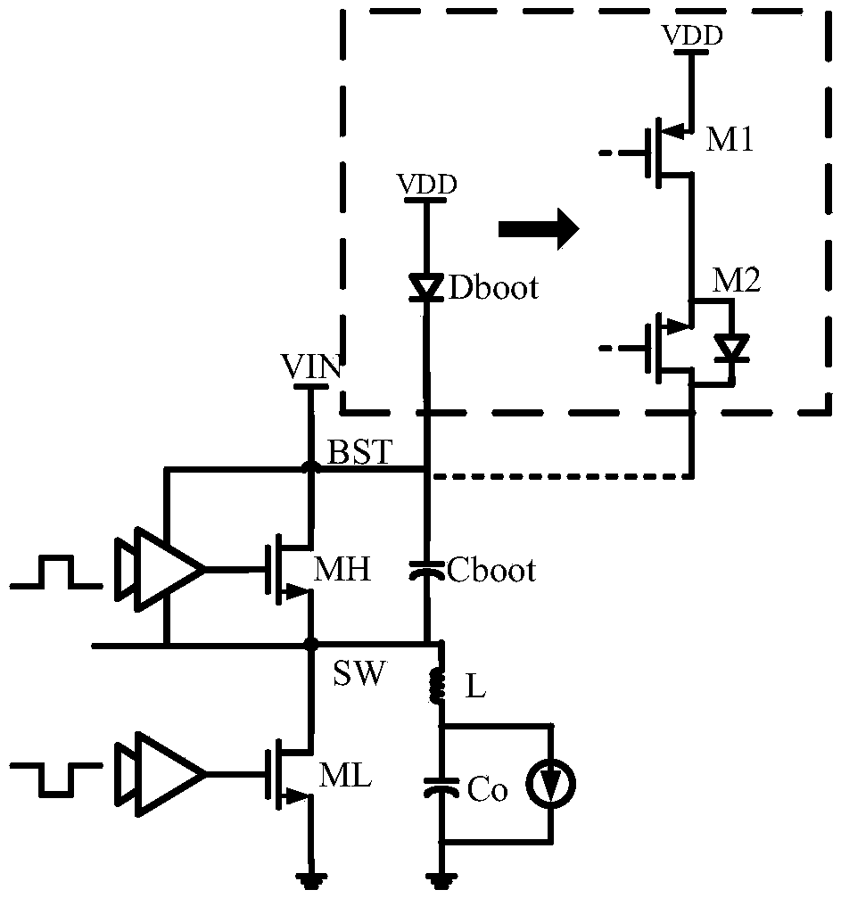
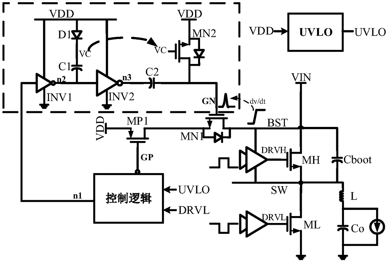
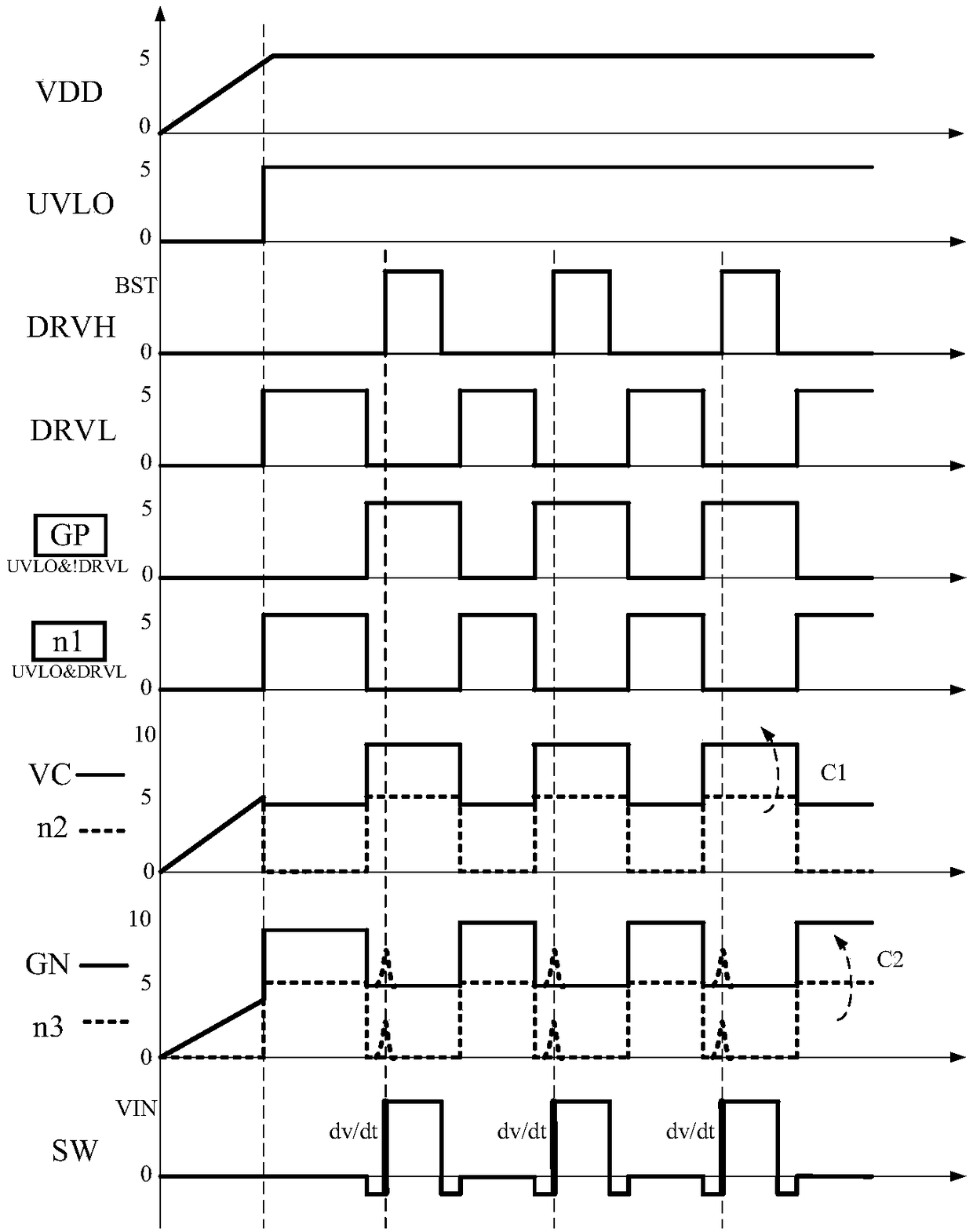
[0021] The switch bootstrap charging circuit proposed by the present invention controls the opening of the bootstrap charging path through the double switch structure composed of the first NMOS transistor MN1 and the first PMOS transistor MP1, and uses the dual charge pump circuit composed of the first capacitor C1 and the second capacitor C2 The first NMOS transistor MN1 is controlled to be turned on, and the first NMOS transistor MN1 is used to replace the bootstrap diode Dboot in the traditional bootstrap charging circuit. The present invention can be applicable to high-speed gate driving of GaN power devices. It is worth noting that the system control mode and specific circuit design used in the present invention can also be applied to Si power switching devices and other wide bandgap semiconductor switching devic...


PUM


Abstract

A switch bootstrap charging circuit suitable for high-speed gate driving of a GaN power device belongs to the technical field of power management. A control logic module generates a first control signal and a second control signal according to the undervoltage signal and the low-side gate driving signal. The gate electrode of the first PMOS transistor is connected to the second control signal, thesource electrode thereof is connected to the supply voltage, and the drain electrode thereof is connected to the source electrode of the first NMOS transistor. An input end of the first inverter is connected with a first control signal, an output end of the first inverter is connected with an input end of the second inverter and is connected with a cathode of the first diode and a gate electrodeof the second NMOS transistor through a first capacitor; The anode of the first diode and the source of the second NMOS transistor are connected to a supply voltage; The gate electrode of the first NMOS transistor is connected to the drain electrode of the second NMOS transistor and is connected to the output end of the second inverter through the second capacitor, and the drain electrode of the second NMOS transistor serves as the output end of the switch bootstrap charging circuit. The invention can prevent the voltage on the bootstrap capacitor from being too large when charging, can realize on-chip integration, and has a simple circuit structure and high reliability. It is especially suitable for GaN high-speed gate drive.

Description

technical field [0001] The invention belongs to the technical field of power supply management, and in particular relates to a switch bootstrap charging circuit suitable for high-speed gate driving of GaN power devices. Background technique [0002] In recent years, the application requirements for high-frequency and high-density power converters have been increasing, and the solutions of traditional silicon technology are constantly facing the challenges of application requirements. On the other hand, GaN power switching devices (such as GaN HEMT high electron mobility transistors) show strong competitiveness due to their small gate charge Qg, no reverse recovery effect, and high voltage resistance, which can allow them to be used in Higher efficiency power conversion at higher switching frequencies. [0003] like figure 1 For the traditional bootstrap charging circuit suitable for silicon Si power switching devices, the bootstrap capacitor Cboot supplies power to the hig...

Claims


Application Information

Patent Timeline
Patent Type & Authority Applications(China)
IPC IPC(8): H02M3/07H02J7/00H03K19/003H03K19/084
CPCH02J7/007H02M3/07H03K19/00369H03K19/084Y02B70/10
Inventor 明鑫潘溯辛杨立张宣胡黎秦尧张春奇王卓张波
Owner UNIV OF ELECTRONICS SCI & TECH OF CHINA
Why Eureka
Try Eureka