

Optical module
a technology of optical modules and optical elements, applied in the field of optical modules, can solve the problems of loss due to intervals between elements, increase in volume, and yield decline, and achieve the effect of small volume, manufacturing and miniaturization
- Summary
- Abstract
- Description
- Claims
- Application Information
AI Technical Summary
Benefits of technology
Problems solved by technology
Method used
Image

Examples
first embodiment
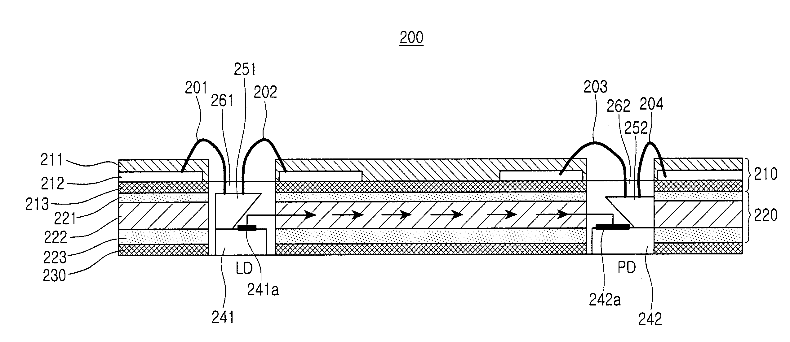
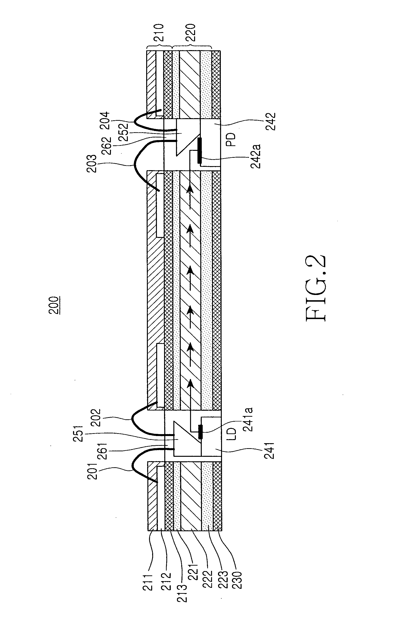
[0023]FIG. 2 illustrates an optical module 200 according to the present invention. As shown, the optical module 200 includes a lower board 230, a light source 241 for generating an optical signal, a waveguide 220 on the lower board 230 for waveguiding the optical signal, a photodetector 242 for detecting the optical signal, a first reflecting mirror 251 on the light source 241 for reflecting the optical signal generated by the light source 241 to a side of the waveguide 220, a second reflecting mirror 252 on the photodetector 242 for reflecting the optical signal emitted from the waveguide 220 in a vertical downward direction, a Printed Circuit Board (PCB) 210 on the waveguide 220, and a plurality of grooves extending from the PCB 210 to the lower board 230.
[0024]FIGS. 3A through 3D illustrate steps of manufacturing the optical module 200. Referring to FIG. 3A, the waveguide 220 is formed on the lower board 230, and the PCB 210 is formed on the waveguide 220. The waveguide 220 inclu...
second embodiment
[0031]FIG. 4 illustrates an optical module 300 according to the present invention. As shown, the optical module 300 includes a lower board 330, a light source 341 for generating an optical signal, a waveguide 320 on the lower board 330 for waveguiding the optical signal, a photodetector 342 for detecting the optical signal, a reflecting mirror 351 on the photodetector 342 for reflecting an optical signal emitted from the waveguide 320 in a vertical downward direction, and a PCB 310 on the waveguide 320, and a plurality of grooves extending from the PCB 310 to the lower board 330.
[0032]The waveguide 320 includes a lower clad 323, a core 322, and an upper clad 321, and emits an optical signal incident through the cleavage surface of its side through the cleavage surface of its other side. The PCB 310 includes driving circuit patterns for driving the light source 341 and the photodetector 342, and a protecting layer may be formed on the PCB 310. The driving circuit patterns are electri...
third embodiment
[0034]FIG. 5 illustrates an optical module 400 according to the present invention. As shown, the optical module 400 includes a first PCB 410, a second PCB 430, a light source 441 for generating an optical signal, a waveguide 420 between the first PCB 410 and the second PCB 430 for waveguiding the optical signal, a photodetector 442 for detecting the optical signal, a first reflecting mirror 451 on the light source 441 for reflecting the optical signal generated by the light source 441 to a side of the waveguide 420, and a second reflecting mirror 452 on the photodetector 442 for reflecting the optical signal emitted from the waveguide 420 in a vertical downward direction. The light source 441 and the photodetector 442 are positioned such that their light emitting surface 441a and light receiving surface 442a face the opened upper portions of the corresponding grooves. Refractive index matching materials 461 and 462 are applied around the light source 441 and the photodetector 442.
[0...
PUM
 Abstract
Description
Claims
Application Information