Substrate processing apparatus and substrate processing method

a substrate processing and substrate technology, applied in the direction of instruments, fluid pressure measurement, coatings, etc., can solve the problems of difficult control, etching rate, etching rate,

Inactive Publication Date: 2007-08-16
TOKYO ELECTRON LTD
View PDF5 Cites 379 Cited by
  • Summary
  • Abstract
  • Description
  • Claims
  • Application Information

AI Technical Summary

Benefits of technology

[0009] It is an object of the present invention to provide a substrate processing apparatus and a substrate pr

Problems solved by technology

As a result, it is difficult to control the flow of the processing gas jetted out from the whole of the surface of the shower head facing the wafer, and hence an etching rate (hereinafter referred to merely as “etch rate”) distribution over the wafer becomes ununiform.
As a result,

Method used


Image

  • Substrate processing apparatus and substrate processing method
  • Substrate processing apparatus and substrate processing method
  • Substrate processing apparatus and substrate processing method

Examples


example 1

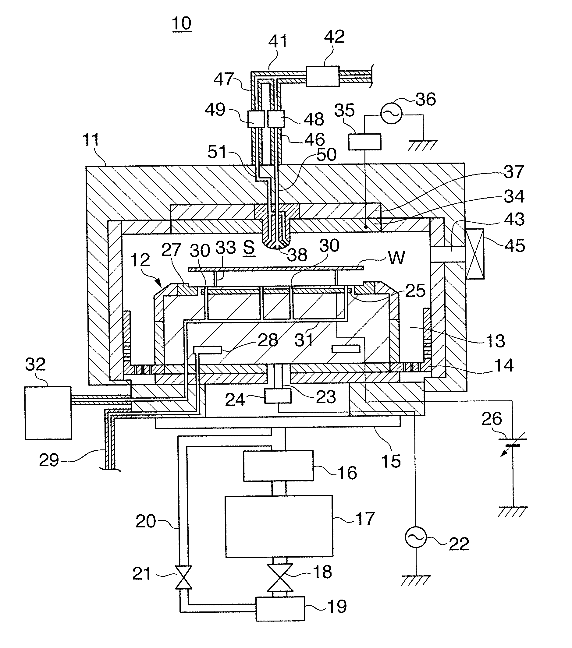
[0084] First, as a wafer to be subjected to etching, a polysilicon film blanket wafer Wb (a wafer having a polysilicon film on a surface thereof formed like a blanket) was prepared. Next, as shown in FIG. 3A, the prepared blanket wafer Wb was transferred into the chamber 11 of the plasma processing apparatus 10, and a mixed gas obtained by adding O2 gas and an inert gas such as He to a brominated gas or a chlorinated gas was supplied as a processing gas into the processing space S in the chamber 11 from the processing gas introducing nozzle 38 in all directions into the processing space S. At this time, the flow rate of the processing gas jetted out into the processing space S by the central portion processing gas introducing hole group, and the flow rate of the processing gas jetted out into the processing space S by the peripheral portion processing gas introducing hole group were equal. Next, radio frequency electrical power was applied into the processing space S so as to produc...

example 2

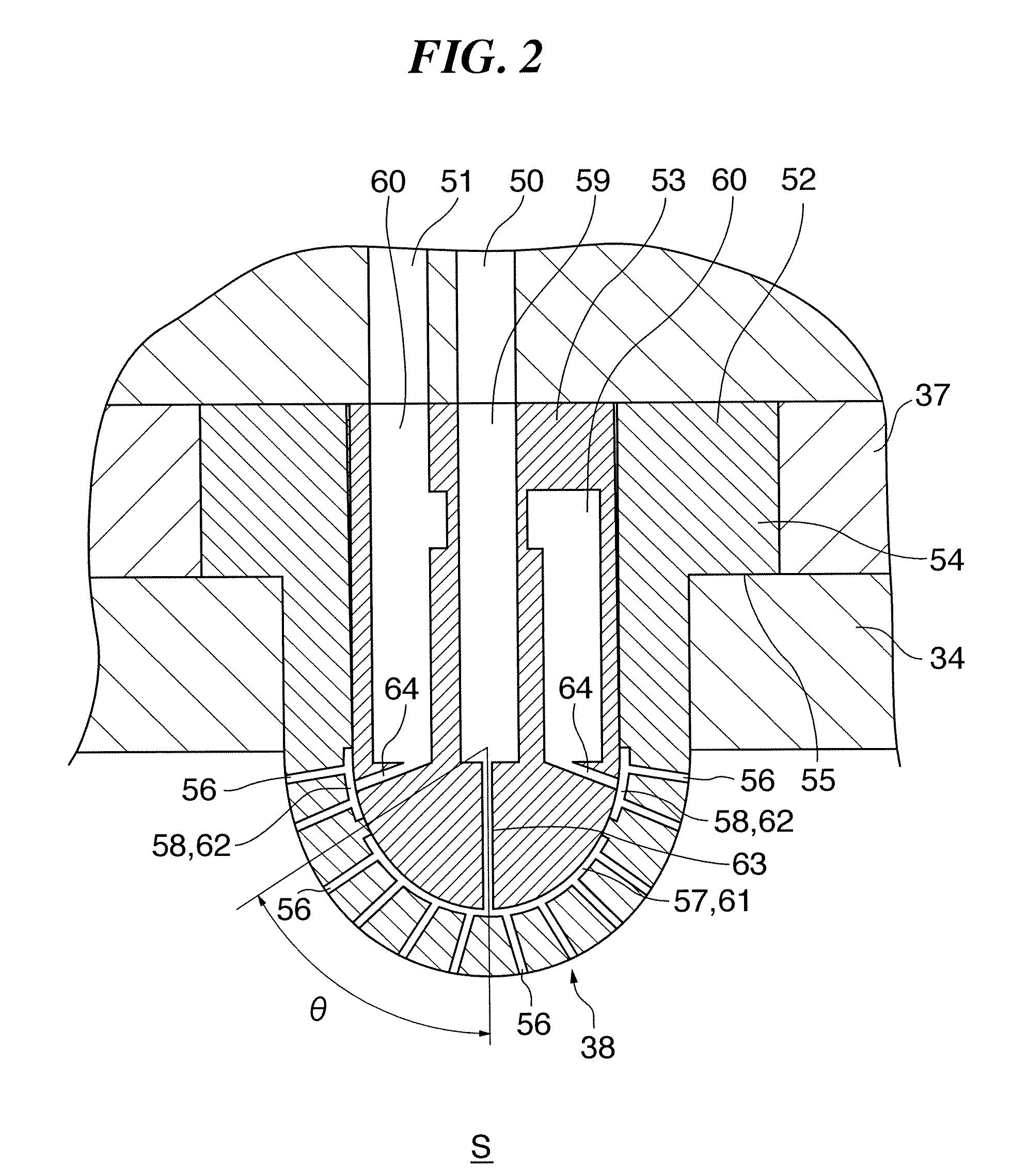
[0093] The apex angle of the above cone was set to 120°, the ratio between the flow rate of the processing gas introduced from the central portion processing gas introducing hole group (CNT) and the flow rate of the processing gas introduced from the peripheral portion processing gas introducing hole group (EDG) was set to 0:100, and a simulation of the flow line distribution in the processing space under this condition was carried out. The results of the simulation are shown in FIG. 6A. The flow line distribution is shown using contour lines in FIG. 6A. Moreover, the above ratio was set to each of 25:75, 50:50, and 75:25, and a similar simulation was carried out under each of these conditions; the results are shown respectively in FIGS. 6B, 6C, and 6D.

example 3

[0101] First, the width of the lowermost portion of the krypton fluoride resist layer 69 on a wafer was measured at a plurality of measurement points along two mutually orthogonal diametral directions (an x-direction and a y-direction) on the surface of the wafer.

[0102] After that, the wafer was transferred into the chamber 11, a mixed gas comprised of CF4, CH2F2, O2, and Ar was supplied as a processing gas into the processing space S from the processing gas introducing nozzle 38, and the pressure in the chamber 11 was set to 4.67 Pa (35 mTorr). Moreover, radio frequency electrical powers supplied from the lower electrode radio frequency power source 22 and the upper electrode radio frequency power source 36 were set to 1000 W and 75 W respectively. As a result, plasma was produced, and the ARC layer 68 was etched by the plasma.

[0103] Next, a mixed gas comprised of HBr, He, and O2 was supplied as a processing gas into the processing space S from the processing gas introducing nozz...


PUM

PropertyMeasurementUnit
Angleaaaaaaaaaa
Angleaaaaaaaaaa
Flow rateaaaaaaaaaa

Abstract

A substrate processing apparatus that enables a state of plasma over a substrate to be maintained in a desired state easily. A plasma processing apparatus 10 that has therein a camber 11, a stage 12, and a processing gas introducing nozzle 38 carries out etching on a wafer W. The chamber 11 houses the wafer W. The stage 12 is disposed in the chamber 11 and the wafer W is mounted thereon. The processing gas introducing nozzle 38 is a projecting body that projects out into the chamber 11, and has therein a plurality of processing gas introducing holes 56 that open out in different directions to one another.

Description

BACKGROUND OF THE INVENTION [0001] 1. Field of the Invention [0002] The present invention relates to a substrate processing apparatus and a substrate processing method, and in particular relates to a substrate processing apparatus that introduces a processing gas into a processing chamber, and carries out plasma processing on a substrate using plasma produced from the introduced processing gas. [0003] 2. Description of the Related Art [0004] A substrate processing apparatus that carries out plasma processing such as etching on a wafer as a substrate has a processing chamber in which the wafer is housed and inside which the pressure can be reduced, a processing gas introducing unit that introduces a processing gas into the processing chamber, and a lower electrode that applies radio frequency electrical power into the processing chamber (a processing space) into which the processing gas has been introduced, and also acts as a stage on which the wafer is mounted. In such a substrate p...

Claims


Application Information

Patent Timeline
IPC IPC(8): G01L21/30H01L21/306C23F1/00C23C16/00
CPCH01J37/32449H01J37/3244
Inventor OKA, HIROMISHIMIZU, AKITAKAENDOH, SHOSUKEDENPOH, KAZUKI
Owner TOKYO ELECTRON LTD
Why Eureka
Try Eureka