Charged particle beam apparatus, charged particle beam focusing method, microstructure measuring method, microstructure inspecting method, semiconductor device manufacturing method, and program

a charge particle and beam technology, applied in the field of charge particle beam apparatus, can solve problems such as shape variation, device properties susceptible, and change in quality

Inactive Publication Date: 2007-08-16
TOSHIBA MEMORY CORP
View PDF4 Cites 11 Cited by
  • Summary
  • Abstract
  • Description
  • Claims
  • Application Information

AI Technical Summary

Benefits of technology

[0043] According to a sixth aspect of the present invention, there is provided a program for a charged particle beam apparatus comprising a control computer, the program being stored in a medium readable by the control computer of the charged particle beam apparatus, the charged particle beam apparatus generating a charged particle beam and then converging the charged particle beam by at least one of an electric field an

Problems solved by technology

However, there are some materials constituting the device which have properties susceptible to the influence of the electron beam application.
These materials not only change their qualities due to the electron beam, but also cause shape variations such as a volume shrinkage.
Thus, the shape of the device pattern changes in an application area where the electron beam has been applied to carry out a measurement or observation, and there is therefore the possibility that the pattern dimensions and the thickness of the film depart from specified values leading to the deterioration of the device performance.
However, all the focusing methods mentioned above repeatedly scan the same place while changin

Method used


Image

  • Charged particle beam apparatus, charged particle beam focusing method, microstructure measuring method, microstructure inspecting method, semiconductor device manufacturing method, and program
  • Charged particle beam apparatus, charged particle beam focusing method, microstructure measuring method, microstructure inspecting method, semiconductor device manufacturing method, and program
  • Charged particle beam apparatus, charged particle beam focusing method, microstructure measuring method, microstructure inspecting method, semiconductor device manufacturing method, and program

Examples


first embodiment

(i) FIRST EMBODIMENT

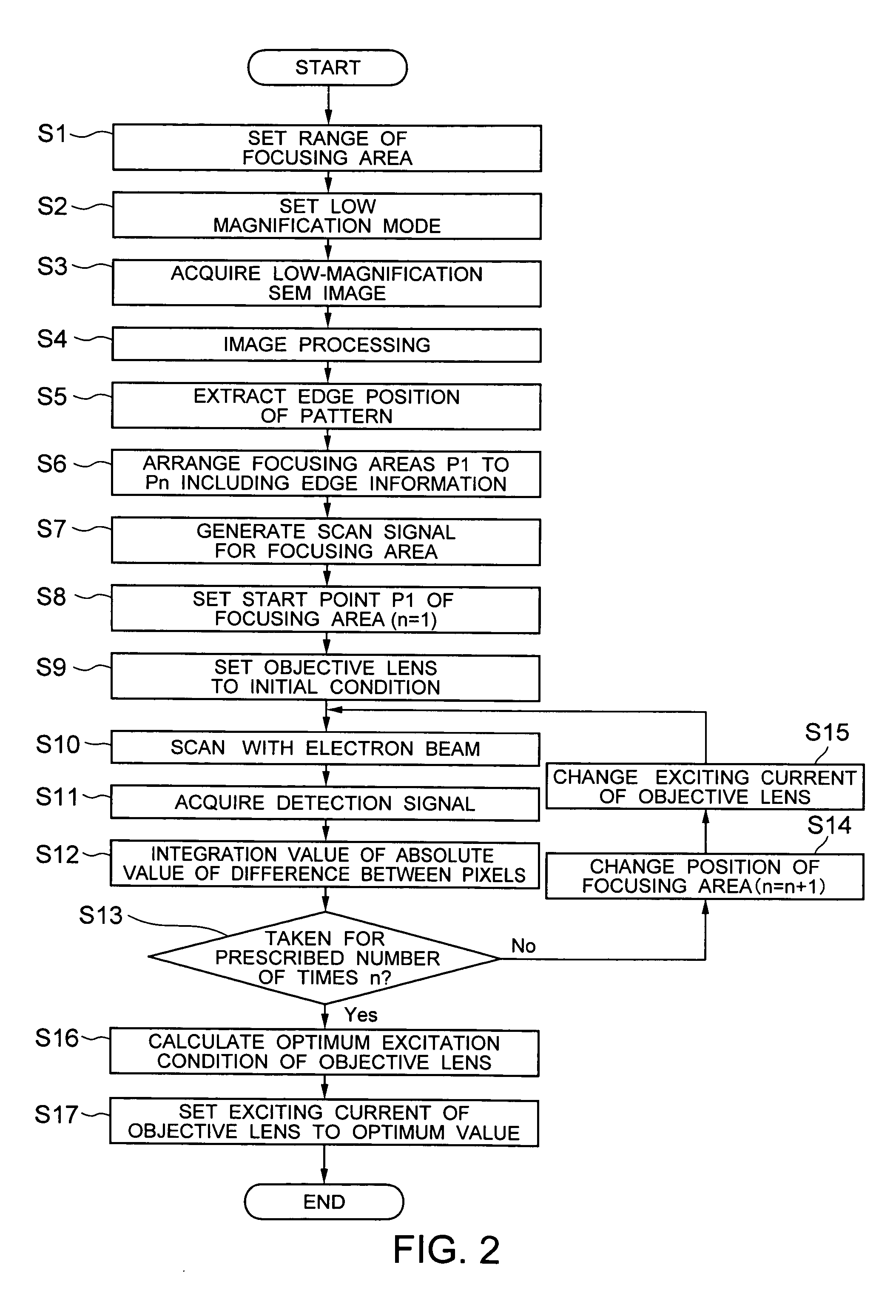
[0066]FIG. 2 is a flowchart showing specific procedures in a first embodiment of a focusing method according to the present invention. FIGS. 3A to 3D are explanatory diagrams showing one example of the arrangement of focusing areas in an edge position. FIGS. 4A to 4C are explanatory diagrams showing specific examples of methods of scanning the focusing area. FIGS. 5A to 5C are explanatory diagrams showing one example of the focusing method to calculate an optimum focal position while changing an exciting current of an objective lens. FIG. 6 is an explanatory diagram of a method of processing by excitations under a plurality of conditions in each of the focusing areas.

[0067] First, the range of the focusing area is set (FIG. 2, step SI). A schematic diagram of the focusing area is shown in FIG. 3A. The range of this area is defined by a horizontal size (Δx) and a vertical size (Δy).

[0068] When the electron beam EB is only applied to the edge of the pattern, the ...

second embodiment

(ii) SECOND EMBODIMENT

[0079] While focusing areas are set in the positions of a pattern edge in the first embodiment described above, the present embodiment is characterized in that the focusing areas are set not in the edge positions but in patterns having a characteristic shape. This enables an arbitrary pattern shape to be focused. FIG. 7 shows a flowchart showing specific procedures in the present embodiment, and FIGS. 8A to 8D show one example of a method of arranging focusing areas in the positions of the pattern having the characteristic shape. In the procedures shown in FIG. 7, the procedures shown in step numbers S21, S24 to S26 are characteristic procedures in the present embodiment, and other procedures are substantially the same as the procedures shown in FIG. 2, and these correspond to the step numbers in FIG. 2 to which 20 is added. Therefore, the procedures different from those in FIG. 2 are mainly described below.

[0080] First, a pattern having a characteristic shape...


PUM


Abstract

A charged particle beam apparatus includes: a charged particle source which generates a charged particle beam and which applies the charged particle beam to a specimen having a microstructure formed on a surface thereof; an objective lens which excites at least one of an electric field and a magnetic field to converge the charged particle beam onto the specimen; a deflector which scans the specimen with the charged particle beam; a detector which detects at least one of a secondary charged particle, a reflection charged particle and a back scattering charged particle generated from the specimen by the application of the charged particle beam and which outputs a detection signal; a focusing area arranging unit which arranges a plurality of focusing areas including edge points of the microstructure therein in a surface area of the specimen; deflection controller which controls the deflector so that the focusing areas are sequentially scanned to correspond to excitation conditions while changing stepwise the excitation conditions, the excitation conditions being conditions for the objective lens to excite at least one of the electric field and the magnetic field; focus calculator which calculates an index indicating a convergence state in each excitation condition on the basis of the detection signal outputted by the detector for the excitation conditions and the focusing areas and which calculates an optimum excitation condition providing an optimum focal position from the obtained index; and an objective lens controller which drives the objective lens under the optimum excitation condition.

Description

CROSS REFERENCE TO RELATED APPLICATION [0001] This application claims benefit of priority under 35 USC §119 to Japanese patent application No. 2006-14902, filed on Jan. 24, 2006, the contents of which are incorporated by reference herein. BACKGROUND OF THE INVENTION [0002] 1. Field of the Invention [0003] The present invention relates to a charged particle beam apparatus, a charged particle beam focusing method, a microstructure measuring method, a microstructure inspecting method, a semiconductor device manufacturing method, and a program. The present invention is directed to, for example, an inspection, observation, etc. of a microstructure such as a semiconductor device, a photomask or liquid crystal device by use of a charged particle beam. [0004] 2. Related Background Art [0005] Various charged particle beam apparatuses are used to observe and evaluate a minute pattern of a semiconductor device, and one representative device is a scanning electron microscope (SEM). The scanning...

Claims


Application Information

Patent Timeline
IPC IPC(8): G21K7/00
CPCH01J37/21H01J2237/2817H01J2237/216H01J37/28
Inventor ABE, HIDEAKIMOTOKI, HIROSHI
Owner TOSHIBA MEMORY CORP
Why Eureka
Try Eureka