Patterned electroless metallization processes for large area electronics

a metallization process and electroless technology, applied in the direction of liquid/solution decomposition chemical coating, natural mineral layered products, coatings, etc., can solve the problems of electroless plating and electrochemical plating having negative effects, poor adhesion to the substrate surface, and debonding of metal layers from the substrate surfa

Inactive Publication Date: 2007-08-16
APPLIED MATERIALS INC
View PDF33 Cites 295 Cited by
  • Summary
  • Abstract
  • Description
  • Claims
  • Application Information

AI Technical Summary

Benefits of technology

[0011] Embodiments of the invention further provide a method of forming a conductive feature on the surface of a substrate, comprising depositing a liquid coupling agent that contains a metal oxide precursor on a surface of a substrate, reducing the metal oxide precursor using a reducing agent, and depositing a conductive layer on the ruthenium containing layer using an electroless deposition process.

Problems solved by technology

Metallization of flat panel display devices, solar cells, and other electronic devices using conventional techniques, such as electroless plating and electrochemical plating have some negative characteristics, which often include poor adhesion to the substrate surface.
Therefore, during the formation of interconnecting layer, such as a copper layer over films deposited using conventional techniques, the intrinsic or extrinsic stress of the deposited layers often lead to debonding of the metal layers from the surface of the substrate.
Also, conventional deposition technologies, such as physical vapor deposition (PVD) and electrochemical metallization processes cannot be used to selectively form metallized features on the surface of a substrate.
To form discrete features using non-selective deposition processes will require the steps of lithographic patterning and metal etch steps to achieve the desired conductive pattern on the substrate surface, which are often cost prohibitive, time intensive, and / or labor intensive.

Method used


Image

  • Patterned electroless metallization processes for large area electronics
  • Patterned electroless metallization processes for large area electronics
  • Patterned electroless metallization processes for large area electronics

Examples


Embodiment Construction

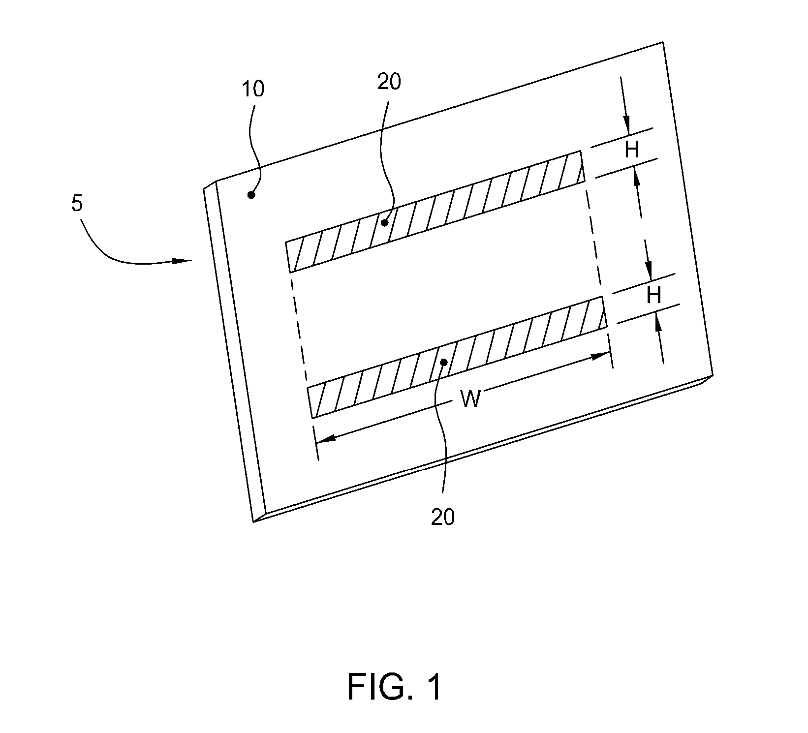
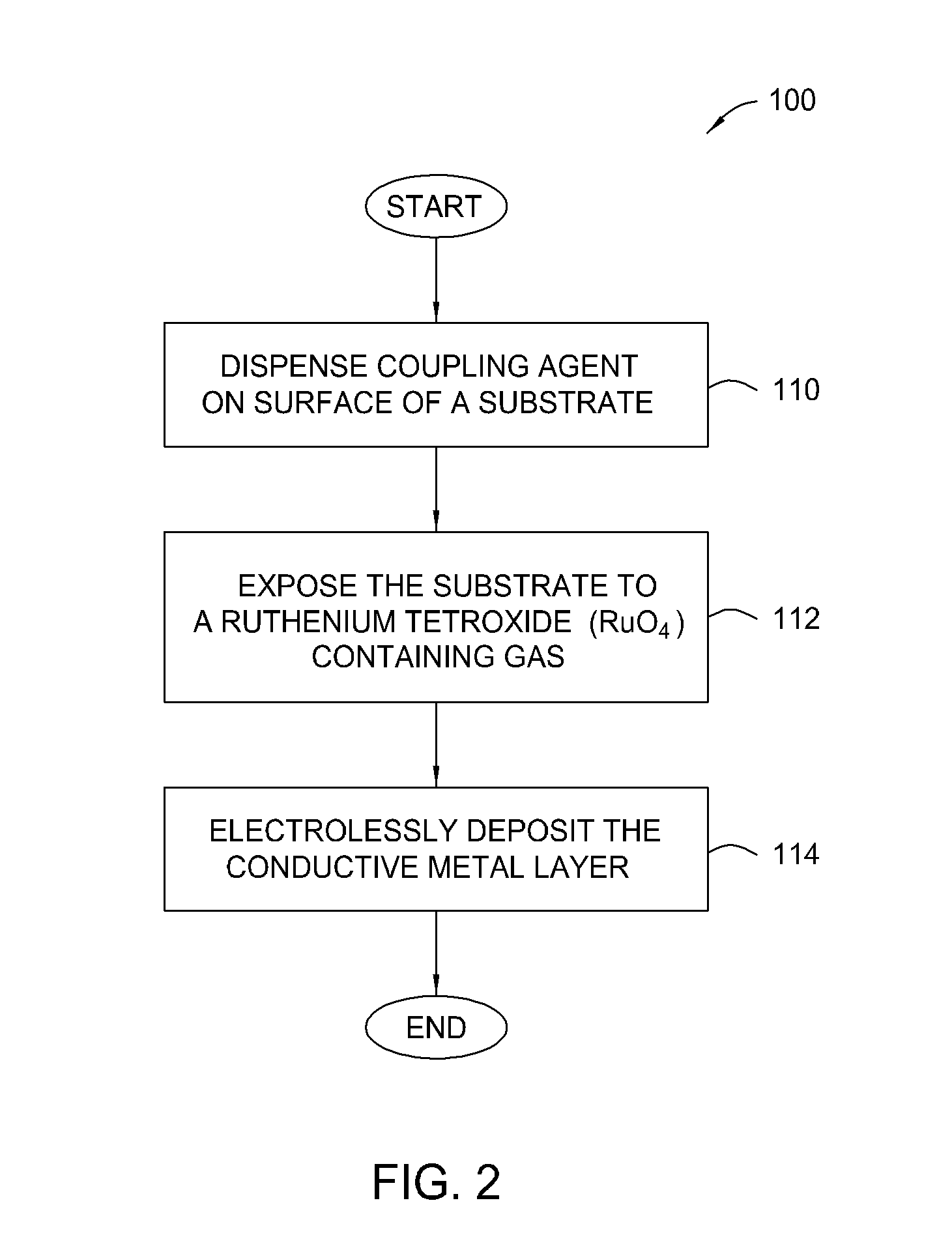
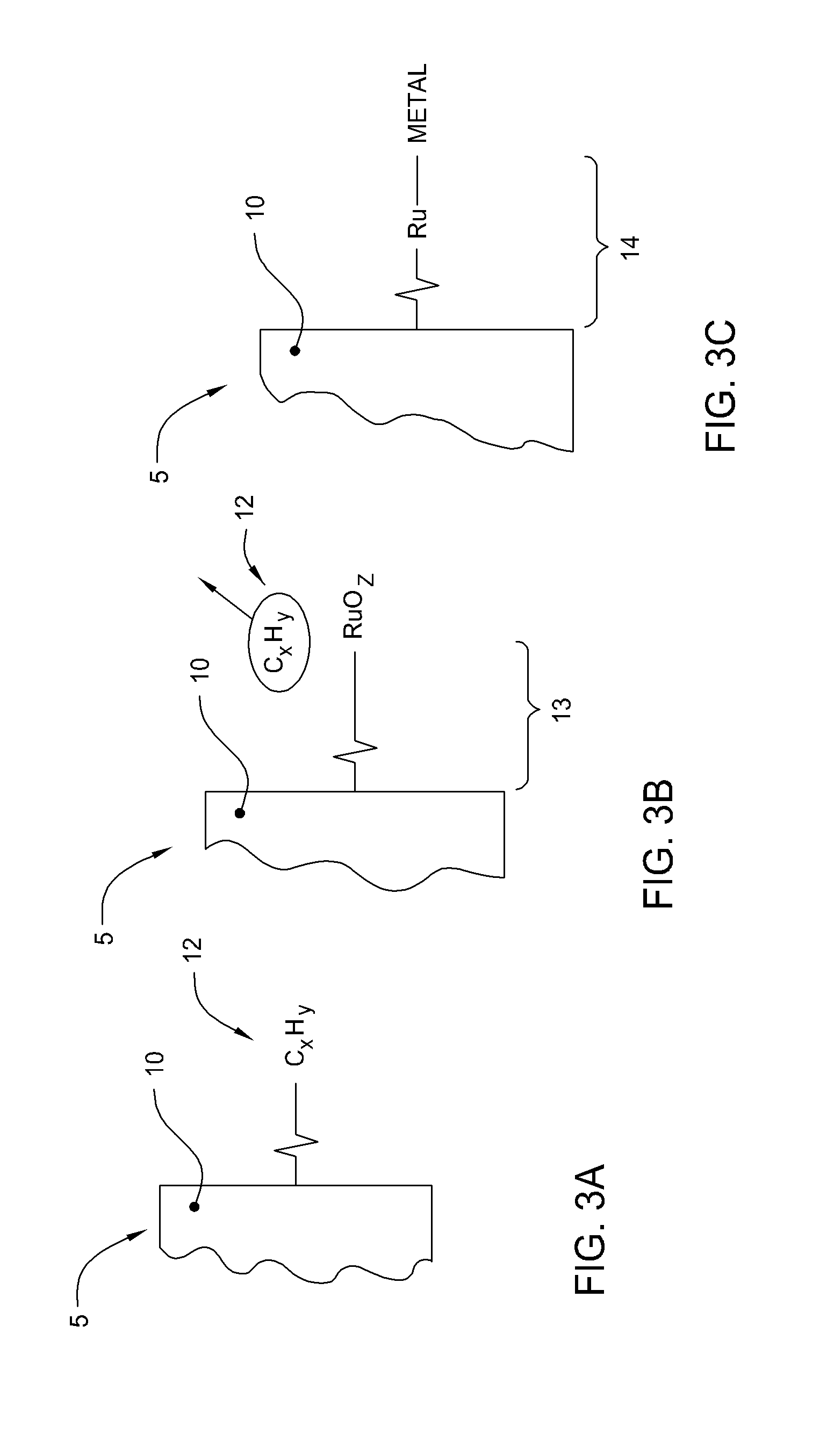
[0028] The present invention generally provides an apparatus and method for selectively forming a metallized feature, such as an electrical interconnect feature, on a electrically insulating surface of a substrate. In general, aspects of the present invention can be used for flat panel display processing, semiconductor processing, solar cell processing, or any other substrate processing. This invention may be especially useful for the formation of electrical interconnects on the surface of large area substrates where the line sizes are generally larger than semiconductor devices (e.g., nanometer range) and / or where the formed feature are not generally as dense. Other features of the invention make it advantageous as a means to apply robust, adherent blanket conductive layers (or precursors to conductive layers) over an entire substrate, as is particularly the case when it is desired to coat complex three dimensional topographies with a uniform conformal coating. The invention is ill...


PUM

PropertyMeasurementUnit
temperatureaaaaaaaaaa
surface areaaaaaaaaaaa
pressureaaaaaaaaaa

Abstract

The present invention generally provides an apparatus and method for selectively forming a metallized feature, such as an electrical interconnect feature, on a electrically insulating surface of a substrate. The present invention also provides a method of forming a mechanically robust, adherent, oxidation resistant conductive layer selectively over either a defined pattern or as a conformal blanket film. Embodiments of the invention also generally provide a new chemistry, process, and apparatus to provide discrete or blanket electrochemically or electrolessly platable ruthenium or ruthenium dioxide containing adhesion and initiation layers. In general, aspects of the present invention can be used for flat panel display processing, semiconductor processing, solar cell device processing, or any other substrate processing, being particularly well suited for the application of stable adherent coating on glass as well as flexible plastic substrates. This invention may be especially useful for the formation of electrical interconnects on the surface of flat panel display or solar cell type substrates where the line sizes are generally larger than semiconductor devices or where the formed feature are not generally as dense.

Description

CROSS-REFERENCE TO RELATED APPLICATIONS [0001] This application claims the benefit of the U.S. Provisional Patent Application Ser. No. 60 / 715,024, filed Sep. 8, 2005, which is herein incorporated by reference.BACKGROUND OF THE INVENTION [0002] 1. Field of the Invention [0003] Embodiments of the invention generally relate to methods for depositing a catalytic layer on a surface of a substrate, prior to depositing a conductive layer thereon. [0004] 2. Description of the Related Art [0005] Metallization of flat panel display devices, solar cells, and other electronic devices using conventional techniques, such as electroless plating and electrochemical plating have some negative characteristics, which often include poor adhesion to the substrate surface. Therefore, during the formation of interconnecting layer, such as a copper layer over films deposited using conventional techniques, the intrinsic or extrinsic stress of the deposited layers often lead to debonding of the metal layers ...

Claims


Application Information

Patent Timeline
Patent Type & Authority Applications(United States)
IPC IPC(8): B05D5/12C23C16/00B05D3/00B05D7/00B32B9/00
CPCB82Y30/00H01L31/0512C23C14/024C23C14/04C23C14/08C23C14/228C23C16/0272C23C16/04C23C16/40C23C18/1608C23C18/165C23C18/1893C23C18/2086C23C18/30C23C18/31H01L21/28556H01L21/28562H01L21/288H01L21/32051H01L21/76838H01L21/76864H01L21/76874H01L31/02008H01L31/022425H05K3/181H05K3/389Y02E10/50C03C17/10B05D7/20
Inventor WEIDMAN, TIMOTHY W.
Owner APPLIED MATERIALS INC
Why Eureka
Try Eureka