Method for fabricating semiconductor devices

a technology for semiconductor devices and manufacturing methods, applied in the direction of semiconductor/solid-state device details, coatings, transistors, etc., can solve the problems of thick gate insulators of misfet, increased time for writing data, and reduced device characteristics

Inactive Publication Date: 2007-08-16
RENESAS ELECTRONICS CORP
View PDF4 Cites 214 Cited by
  • Summary
  • Abstract
  • Description
  • Claims
  • Application Information

AI Technical Summary

Benefits of technology

[0009] An object of the present invention is to provide a technique capable of forming the silicon oxide with the film quality equivalent to that of the thermal oxide without the thermal oxidation in the manufacturing process of a semiconductor device.

Problems solved by technology

However, since the voltage used in the non-volatile memory is high, the gate insulator of the MISFET is thick.
As a result, since some defects occur in the semiconductor substrate and a junction leakage current is increased, there has been the problem that the device characteristics are degraded, for example, the time for writing data is increased due to the decrease of the writing voltage.
However, since the underlying material of such portion is not the semiconductor substrate, it is difficult to form a high-quality silicon oxide by the thermal oxidation method.
However, due to the insufficient effect of the thermal treatment, there has been the problem that it is difficult to obtain the film quality equivalent to that of the thermal oxide.

Method used


Image

  • Method for fabricating semiconductor devices
  • Method for fabricating semiconductor devices
  • Method for fabricating semiconductor devices

Examples


first embodiment

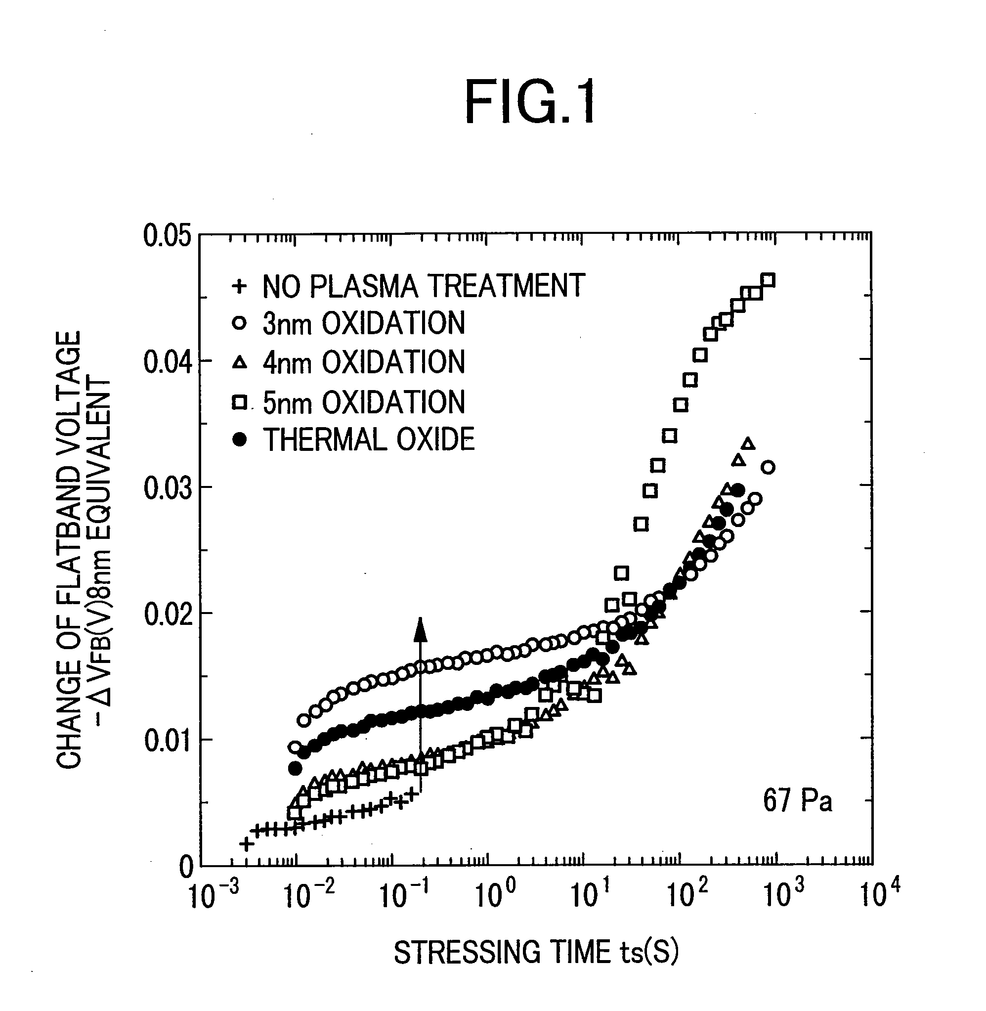
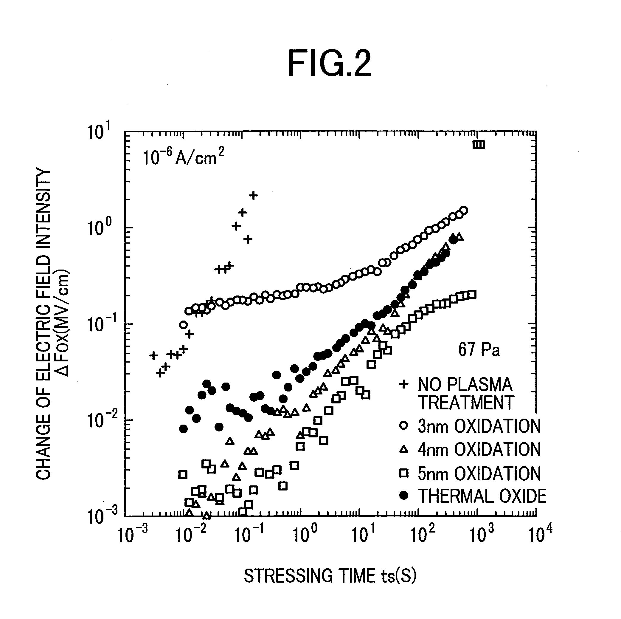
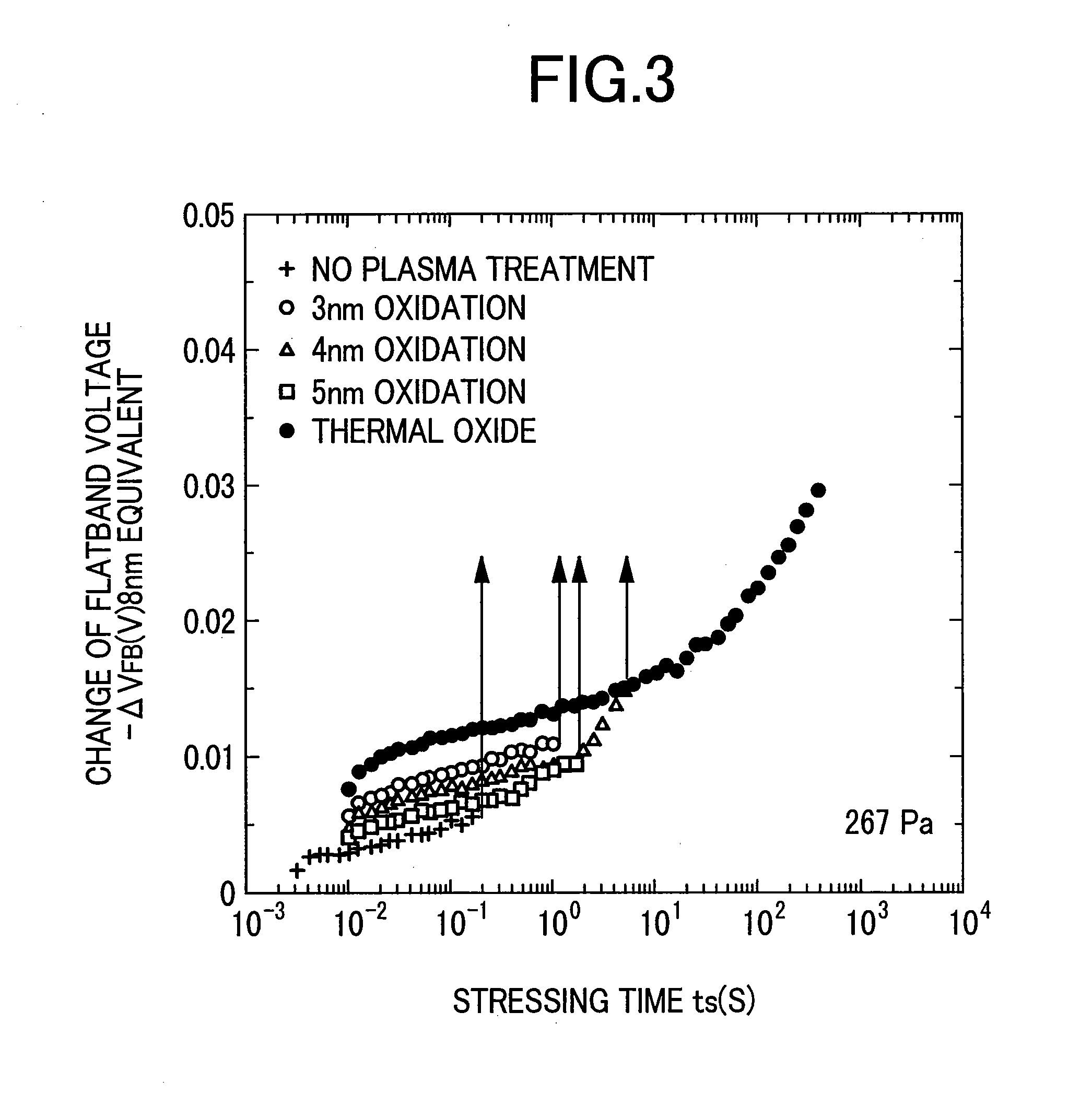
[0180] The inventors have first found out that, when the plasma treatment (oxygen plasma treatment) in an atmosphere containing oxygen (O2) as a main gas is performed to the silicon oxide (SiO2 and the like) deposited by the CVD (Chemical Vapor Deposition) method, the action of the ions in plasma, especially, of oxygen ions (O+ or O2+) is important for the quality improvement of silicon oxide. This is probably because the physical (mechanical) impact by the ions in plasma, collided to the silicon oxide, causes the rearrangement of the constituent atoms in the silicon oxide and, thus, the film quality of the silicon oxide will be improved. Hereinafter, results of the experiment by the inventors for verifying the effectiveness of the embodiments will be described with reference to FIGS. 1 to 10. Note that radical oxygen by plasma is abbreviated to “oxygen radical (O*)”.

[0181] In the experiment of FIGS. 1 and 2, an n type gate MOS capacitor is fabricated and is used as an experiment s...

second embodiment

[0205] In the second embodiment, an example of the case where the gate insulator in the thin-film region is also formed of the CVD oxide film will be described with reference to FIGS. 18 and 19. FIGS. 18 and 19 are sectional views showing the principal part of the semiconductor wafer 2W in the fabrication process of the semiconductor device according to the second embodiment.

[0206] First, after the process of removing the insulator 4 shown in FIG. 12 in the first embodiment, as shown in FIG. 18, an insulator 6b made of, for example, silicon oxide is deposited on the main surface of the semiconductor wafer 2W by the LPCVD method to have about 16 nm in equivalent oxide thickness, and, further, the oxygen plasma treatment similar to that described with reference to FIG. 13 is performed to the insulator 6b. By so doing, the film quality of the insulator 6b formed by the LPCVD can be improved to be equal to that of the silicon oxide formed by the thermal oxidation.

[0207] Next, similarl...

third embodiment

[0209] In a third embodiment, an example of the case where the gate insulator in the thin-film region is formed by the above oxygen plasma treatment will be described with reference to FIGS. 20 to 22. FIGS. 20 to 22 are sectional views showing the principal part of the semiconductor wafer 2W in the fabrication process of the semiconductor device according to the third embodiment.

[0210] First, after the process of removing the insulator 4 shown in FIG. 12 in the first embodiment, as shown in FIG. 20, an insulator 6d made of, for example, silicon oxide 6d is deposited on the main surface of the semiconductor wafer 2W by the LPCVD method to have about 24 nm in equivalent oxide thickness. Subsequently, after forming a resist pattern with an opening in the thin-film region A1, the insulator 6d is selectively removed in the hydrofluoric acid solution with using the resist pattern as an etching mask. Thereafter, after removing the resist pattern and performing the cleaning process, the ox...


PUM

PropertyMeasurementUnit
pressureaaaaaaaaaa
pressureaaaaaaaaaa
voltageaaaaaaaaaa

Abstract

According to the present invention, an oxide film with the film quality almost equivalent to that of the thermal oxide can be formed by the low-temperature treatment. After removing an insulator on the active region of the substrate which constitutes a semiconductor wafer, an insulator made of, for example, silicon oxide is deposited on the main surface of the semiconductor wafer by the low pressure CVD method. This insulator is a film to form a gate insulator of MISFET in a later step. Subsequently, a plasma treatment is performed in an atmosphere containing oxygen (oxygen plasma treatment) to the insulator in the manner as schematically shown by the arrows. By so doing, the film quality of the insulator formed by the CVD method can be improved to the extent almost equivalent to that of the insulator formed of the thermal oxide.

Description

BACKGROUND OF THE INVENTION [0001] The present invention relates to a technique for fabricating a semiconductor device and, more particularly, to a technique effectively applied to a method for forming an insulator, which constitutes the semiconductor device. [0002] Some semiconductor devices include a MISFET (Metal Insulator Semiconductor Field Effect Transistor) in which two or more gate insulators different in thickness are formed on the same semiconductor substrate. In general, the MISFET with a relatively thick gate insulator is used as a high breakdown voltage MISFET to which a relatively high voltage is applied. [0003] In a non-volatile memory such as a flash memory or the like, data is recorded by storing electric charges in an isolated electrode (floating electrode) during the operation of the data writing and deleting. Therefore, high voltage of, for example, about 20 to 26 V is necessary to introduce the electric charges into the floating electrode. For this reason, the g...

Claims


Application Information

Patent Timeline
Patent Type & Authority Applications(United States)
IPC IPC(8): H01L21/76C23C16/56C23C16/42H01L21/28H01L21/3105H01L21/316H01L21/318H01L21/336H01L21/768H01L21/8234H01L21/8238H01L21/8247H01L23/522H01L27/088H01L27/092H01L27/10H01L27/105H01L27/115H01L29/51H01L29/788H01L29/792
CPCH01L21/28185H01L21/28194H01L21/28273H01L21/3105H01L21/823857H01L27/105H01L27/11521H01L2924/0002H01L27/11526H01L29/513H01L29/518H01L2924/00H01L29/40114H10B41/40H10B41/30H01L21/18
Inventor HIRAIWA, ATSUSHISAKAI, SATOSHIISHIKAWA, DAIIKEDA, YOSHIHIRO
Owner RENESAS ELECTRONICS CORP
Why Eureka
Try Eureka